Follow these emi emc principles to prevent your pcb design
- Posted On:
- June 25, 2024
- Category:
- Analysis & Simulation

EMI EMC Analysis
In this crazy high-tech world and the ongoing growth of our planet, it’s super important to remember the basic rules that help us be better people.
When it comes to PCB design, keeping electromagnetic interference (EMI) in check is like ensuring your car runs smoothly—vital for top-notch performance.
By sticking to electromagnetic compatibility (EMC) design principles, PCB designers can dodge the EMI bullet and keep their circuit boards ticking like clockwork.
So, let’s roll up our sleeves and uncover the inside scoop on key principles and tricks straight from our design experiences.
We’re about to give you the backstage pass to mastering EMI prevention in your PCB designs.
Understanding EMI and EMC
Understanding EMI and EMC can be crucial in designing electronic circuits to prevent interference. EMI, or electromagnetic interference, occurs when electronic devices radiate or conduct electromagnetic energy that can cause interference with other devices. To reduce EMI in a printed circuit board (PCB), designers must follow PCB design guidelines for EMI.
This includes ground planes, shields, trace routing, and proper PCB layout design to minimize the amount of EMI that is radiated or conducted.
High-speed signals and power supplies are common sources of EMI, but following good EMC design rules can help to control EMI and prevent EMI issues.
When designing a PCB, it is important to create a layout that reduces the loop area and properly routes the return path to prevent EMI interference.
By following EMC design guidelines and using EMC compliant components, designers can reduce the amount of EMI emissions and ensure good EMC performance.
Keeping EMI in check during the design process is essential to control EMI from both internal and external sources and minimize the piece’s EMI impact on the overall system.
For example, think of a cell phone causing static on a nearby radio. That’s EMI. Now, imagine engineers making sure that the phone and the radio play nice together without causing any static.
That’s EMC analysis in action!
Follow these emi emc key principles to prevent your pcb design
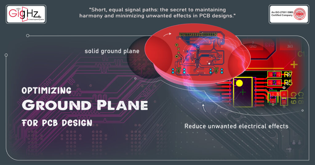
Optimizing Ground Plane for PCB Design
When we talk about reducing EMI (which stands for electromagnetic interference), the ground plane in a PCB plays a really important role. It’s like the bodyguard that ensures all the circuits have the right environment to do their job without causing trouble.
Here are some simple ways to design the ground plane to reduce EMI:
Make it Big:
By making the ground area bigger within the PCB, we can help signals spread out more effectively, which reduces noise and other problems. This is especially helpful in PCBs with multiple layers.
Solid is Better:
A solid ground plane works better than other designs in reducing electrical resistance, which is like the flow of energy. This is important in multi-layer PCBs.
Connect Everything:
It’s crucial to connect every single part of the circuit to the ground plane. This helps neutralize any unwanted effects on the board design.
Be Careful with Different Voltages:
When dealing with different voltages in the circuit, we might need to use split planes to create separate ground areas. But we have to be careful not to create loops that cause EMI.
Use Capacitors Smartly:
Adding specific types of capacitors to the ground plane can help reduce unwanted electrical effects and make everything run smoother.
Keep Things Short and Equal:
Making sure that the paths for the electrical signals are short and equal in length can help prevent unwanted effects and keep everything working well.
Optimizing Trace Layout for Reduced Electromagnetic Interference
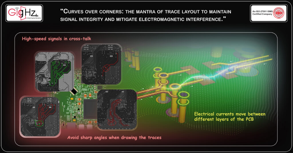
Let’s talk about how to lay out the traces on a PCB in a way that reduces electromagnetic interference. Traces are like the paths for the electrical currents in the circuit, and it’s important to arrange them properly to avoid problems.
Here are some simple rules to follow when laying out traces on a PCB:
Avoid Sharp Angles:
Try to avoid sharp angles when drawing the traces. If the angles are too sharp, it can cause the electrical behavior to change and lead to interference. Instead, make the corners more rounded or use a series of smaller angles.
Keep Different Signals Separate:
It’s a good idea to keep the fast-moving electrical signals away from the slower ones, and to keep the analog signals separate from the digital ones. If they get too close, they can interfere with each other.
Keep Return Paths Short:
The path that the electrical current takes needs to be as short as possible and should follow the easiest route back. This helps to reduce interference.
Mind the Space:
When two high-speed signals run close together, they can interfere with each other through something called cross-talk. To prevent this, it’s important to keep some space between them. Generally, keep them at least twice the trace width apart.
Be Careful with Vias:
Vias are like little tunnels that let the electrical currents move between different layers of the PCB. But we have to be careful when using them, as they can introduce their own effects that cause interference. If we have to use them, we need to plan carefully.
Organizing Electronic Components to Minimize Electromagnetic Interference
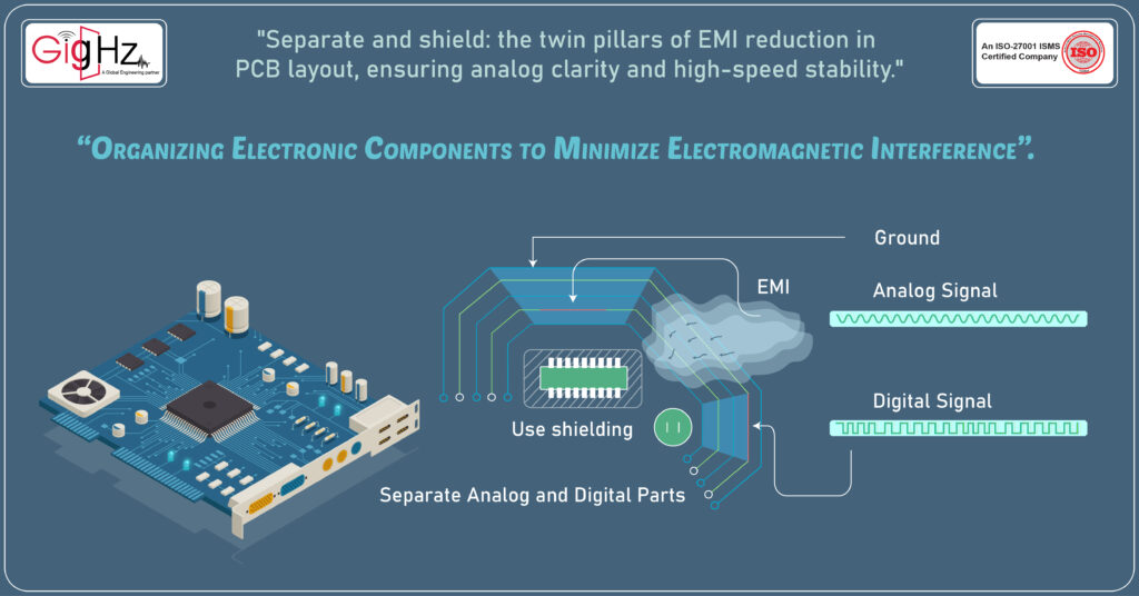
Now, let’s simplify and break down the best practices for arranging electronic components in PCB design to reduce EMI issues,
Separate Analog and Digital Parts:
Just like with the traces, it’s important to keep analog and digital circuits and components separate. If they get too close, they can interfere with each other. To prevent this, we can use different layers and separate grounds to keep them as far apart as possible.
Separate Analog and High-Speed Parts:
Analog circuits carry strong electrical currents, which can cause problems for high-speed signals. It’s best to keep them away from each other and use shielding to protect the analog circuits. On multi-layer PCBs, we can route the analog traces so that there’s a ground plane between the analog circuit and the high-speed signals.
Be Careful with High-Speed Components:
Faster and smaller components tend to produce more EMI. We can deal with this by using shielding and filtering. It’s also a good idea to keep these components away from others on the board. Additionally, keeping high-speed signals and clocks short and close to the ground plane helps control interference and noise levels.
By following these simple guidelines, we can ensure that the arrangement of electronic components in our PCB design minimizes EMI issues and helps everything work together smoothly.
Our Notable Upgrade: Engineering as a Service(EaaS)
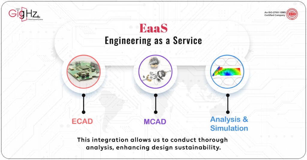
Absolutely! As the demand for advanced engineering solutions keeps growing, our Engineering as a Service (EaaS) is really stepping up its game.
We’re tapping into the power of ECAD, MCAD, and Analysis & Simulation, which positions us as frontrunners in the industry.
The fact that we offer a full package, covering every single step of the engineering process, is what makes our approach so exciting.
It’s this kind of forward-thinking approach that’s going to shape the future of our engineering,
It’s truly thrilling!
Conclusion
So, after diving deep into the world of EMI, EMC, and all things related to PCB design, it’s time to draw a conclusion.
It turns out that the key to a best PCB design is to carefully consider all the possible EMI sources that could disrupt the performance of the PCB.
From EMI radiations to conducted EMI and even EMI from external sources, there are plenty of factors to take into account. By implementing the right circuit design and pcb stackup, it is possible to prevent electromagnetic interference and ensure EMC compliance.
Plus, don’t forget about using design tools to reduce the radiated emissions and power rail noise.
Because let’s face it, too much EMI can result in some effects that no one wants to deal with!
Book a call. Schedule a free consultation now. https://calendly.com/gighz/30min
Follow these emi emc principles to prevent your pcb design
Book a Free Consultation Call
Partner with Gighz and bring your most innovative design concepts to life. Our engineering cad services accelerate development so you can focus on your big vision.
Related Blogs