Professional PCB Designing & Circuit Board Layout Services
PCB designing services means taking your circuit diagrams and schematic designs, and turning them into physical PCB units ready for use in your products. It brings your ideas to life and enables us to manufacture the precise boards you need through end-to-end Circuit Board Design Services.
We design printed circuit boards of any complexity—rigid, flexible, multilayer, HDI boards, high-speed PCBs, and more. Whether starting from scratch or refining an existing electric circuit, our team delivers fast, accurate results using advanced PCB Layout Services and the latest PCB design tools combined with proven design methodologies.
PCB designing services means taking your circuit diagrams and schematic designs, and creating physical PCB units that can be used in your components. It brings your designs to life and enables us to manufacture the precise circuit boards you need.
We design printed circuit boards of any complexity: rigid, flexible, multilayer, HDI boards, high-speed PCBs, and other types. Our team can create boards from scratch or improve an existing electric circuit design. Application of the latest PCB design tools combined with our proven methodologies allows faster design turnaround.
How Does PCB Design Work?
Here are the key steps involved in our PCB designing services
Component Placement – We position components on the board based on schematic layouts, optimizing them for functionality, design rules, and manufacturability as part of our comprehensive Circuit Board Design Services.
Routing -We create copper traces layer-by-layer to interconnect components according to schematic nets and electrical constraints, ensuring accuracy through expert PCB Layout Services.
Verification – This is a crucial step where different layout validations with design rule checks, signal integrity analysis, power integrity analysis and physical testing are performed to identify and correct issues.
Iterations – We then refine and optimize placement and routing to meet all electrical, mechanical, and fabrication requirements.
Our PCB Design Capabilities
We also specialize in
- Layer Stack-up creation
- DFx Compliance
- Smart Signal Routing
- Handled up to 0.37mm BGA pitch designs
- Power route optimization
- Controlled Impedance Matching
- Critical Signal Length Matching
- Length Match report generation
- Attractive routing and clean up
- Designs with Back Drill
Why Choose GigHz For PCB Designing Services
Our top-notch PCB designs features with advanced technologies like PCI and DDRx. We provide prompt and accurate deliveries, with a focus on cost reduction and maximizing potential. Our team knows how to quickly and accurately give you the results you want, by following the standards and guidelines.
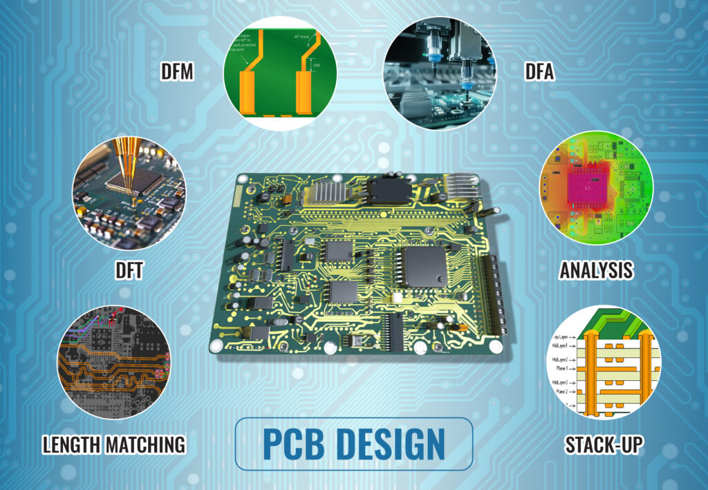
With expertise in compact mixed-signal PCBs, our team ensures prompt and precise results as per specifications. Complicated Design Rule Checks, comprehensive Net Connectivity Verification and Schematic Alignment upholds exceptional quality. Our team also has strong expertise in advanced design methodologies like DFM, DFF, DFA, DFT critical for manufacturability.The availability of a 3D preview and export for mechanical CAD modeling further enriches our services.
Our PCB Designing Process at GigHz
Our PCB Design process follows these typical steps.
- We first collaborate with the client to understand product goals and specifications. If needed, we help define the requirements.
- We then create a high-level board architecture and select components to meet the specifications. This is presented for validation.
- We create the detailed schematics for the board defining all connectivity. Supporting documentation like BoM is provided.
- We layout the board optimizing placement and routing to meet electrical and mechanical needs. Simulation and analysis is done.
- Extensive checks are done to ensure the layout meets schematics and requirements. Issues are identified and resolved.
- Once fully validated, the final board is fabricated and assembled.
- Initial prototypes are tested and validated.
- Comprehensive testing is done before delivering the finished boards to the client.
Do you need help with defining your requirements for the PCB design process?
Book a Call to Schedule a Free Consultation Now.
Q: What are Printed Circuit Board (PCB) Designing Services?
A: Printed Circuit Board (PCB) Design Services involve the process of designing and creating the layout for electronic circuit boards used in various electronic devices. These services cater to a wide range of PCB requirements, from schematic design to product development and testing.
Q: What does a typical PCB Design Service include?
A: A typical PCB Designing Services package includes schematic capture, Circuit Board Design Services, PCB Layout Services, testing, and related offerings such as CAD design, hardware design, and electronic component selection.
Q: What are the advantages of using Professional PCB Design Services?
A: Professional PCB Design Services offer expertise in custom PCB design, high-speed and multi-layer PCB design, rigid-flex PCB design, and the use of leading PCB design tools, ensuring the quality and reliability of the designed circuit boards.
Q: How do PCB Design Services contribute to product development?
A: PCB Design Services play a crucial role in product development by providing PCB board design tailored to the specific needs of the product, including industrial design, mechanical design, and electronic component integration, resulting in a well-integrated product.
Q: What types of electronic products can benefit from PCB Design Services?
A: All types of electronic products, from consumer electronics to industrial equipment, can benefit from PCB Design Services, as they cater to diverse electronic design needs for a wide range of applications.
Q: What is the Difference Between PCB Design and Schematic Design?
A: Schematic design deals with the conceptual and logical representation of the circuit, while PCB design involves the physical implementation of the circuit on a printed circuit board. Schematic design focuses on functionality and connectivity, while PCB design focuses on the layout, routing, and optimization of the physical components and traces on the board. Both stages are crucial in the overall process of electronic circuit development.
Q: How does 8D analysis help in PCB Design?
A: In PCB design, 8D analysis can be applied when defects, quality issues, or field failures occur. It helps the design team methodically analyze root causes and develop corrective and preventive actions.
Q: How can GigHz-EaaS help PCB Design for startups to Enterprise companies?
A: At GigHz, we offer end-to-end PCB design services that provide value for organizations of all sizes, from startups to large enterprises. Our key benefits include:
Expertise – We have experience with complex PCB technologies like PCIe, DDRx, HDI, and high-speed interfaces. This allows us to handle demanding PCB design projects.
Quality – We follow robust design and review processes focused on DFM, DFT, and quality. This results in reliable, manufacturable board designs.
Scalability – We can scale our PCB design team and capacity to suit each client’s project needs, from one-off boards to high-volume programs.