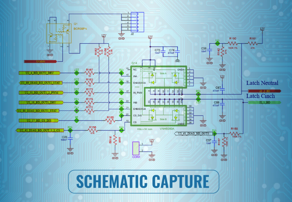
Expert Schematic Capture Design Services
Bringing your electronic product to life starts with a simple yet powerful tool: the PCB Schematic Design. This blueprint is like a map that shows the circuit’s functions and how components are connected — forming the foundation of a reliable Circuit Schematic Design.
Creating a schematic design before the layout stage saves time and money. Our PCB Schematic Capture process ensures accuracy by determining the board’s size, mechanical constraints, and component density. Clearance, routing, connectors, and assembly procedures are also carefully evaluated to guarantee proper fit and function.
The team at GigHz knows how crucial it is to get this step right before moving onto the PCB layout. With decades of experience in ECAD services, we’ve mastered the art of translating complex ideas into functional schematics that get your product off the ground.
Bringing your electronic product to life starts with a simple yet powerful tool: the PCB schematic design. This blueprint is like a map that shows the circuit’s functions and how components are connected to one another.
Creating a schematic design before the PCB layout saves time and money. To ensure proper fit and function, we’ll need to determine the size, mechanical requirements, and component density of the board. Clearance, routing, connectors, and assembly procedures are also critical factors to consider.
The team at GigHz knows how crucial it is to get this step right before moving onto the PCB layout. With decades of experience in ECAD services, we’ve mastered the art of translating complex ideas into functional schematics that get your product off the ground.
Our Schematic Capture Design Services
As a vital step in the hardware design process, PCB Schematic Capture becomes an interaction between designers and specialized tools.
Aligned with your specifications, our team leverages dedicated PCB Schematic Design and refinement tools. We generate compatible netlists for various simulation and Circuit Schematic Design and PCB layout packages, enhancing design adaptability. Additionally, errors in the schematic are rectified through the integration of component datasheets, ensuring precision and reliability.
We also specialize in:
- Manual Schematic Capture
- PCB design services
- Multi-Tier Hierarchical Design
- Schematic Optimization
- Schematic and Layout Integration
- Electrical Rule Checking
- Error-Free Schematics
- Schematic Reuse
- Cable Harness Schematics
Trust our expertise to produce meticulous schematics that seamlessly guide your circuit design from concept to reality.
Multi-Level Hierarchical Schematics
This module of GigHz delivers a number of features for visual and logical pin connections. Cross-module management ensures that principal circuits can be easily converted to PCB, back annotated, or imported/exported from other EDA, CAD, and netlist formats. Verification and SPICE export for simulation allow for full project analysis.
A proper schematic capture design provides the following features.
- Visual and logical structure – Component pins can be connected visually with wires and buses or logically without wires, using net ports, bus ports, or by name
- Electrical Rule Check – Electrical Rule Check with detailed customization reports short circuits, superimposing and unconnected pins, one-pin nets, and checks connections by pin types.
- Import/Export – Our schematic capture design supports import and export of schematic files and drawings with various CAD tools like Altium, Eagle, P-CAD, PADS, OrCAD,Siemens EDA tools,Cadence tools and KiCAD. This allows design data exchange between different schematic editors.
You can provide the schematic data to us in a number of ways either electronically or through paper. We will work closely with your design team to ensure that the correct functionality is captured accurately and effectively.
Need to Discuss? Book a Free Call Here!
Q: What are schematic capture design services?
A: Schematic capture design services involve creating a graphical representation of an electronic circuit using specialized software. This process includes drawing the circuit, adding components, and connecting the parts to define the electrical connections and functionality.
Q: What is PCB design?
A: PCB design, also known as printed circuit board design, is the process of creating the layout and routing for electronic components on a PCB to ensure proper functionality and electrical connections.
Q: How can schematic capture and PCB layout services benefit my project?
A: Utilizing schematic capture and PCB layout services can streamline the design process, ensure accurate electrical connections, optimize board space, and ultimately lead to a more efficient and functional electronic product.
Q: What are primary tasks conducted by design engineers in the context of hardware design?
A: Design engineers involved in hardware design are responsible for tasks such as schematic entry, PCB layout, component selection, signal integrity analysis, and ensuring that the hardware meets the intended specifications and performance requirements.
Q: What is the role of schematic symbols in electronic design?
A: Schematic symbols represent components in circuit diagrams. They are essential for accurate PCB Schematic Capture, effective PCB Schematic Design, and clear Circuit Schematic Design, ensuring proper connectivity and communication in electronic systems.
Q: How can PCB design software such as Altium Designer contribute to the design process?
A: PCB design software like Altium Designer offers advanced features for schematic and PCB design, component management, rule checking, signal integrity analysis, and 3D modeling, which can significantly enhance the efficiency and accuracy of the design process.
Q: How can GigHz-EaaS help schematic creation for startups to Enterprise companies?
A: GigHz offers end-to-end schematic design services that provide benefits for organizations of any size:
Domain expertise – Our engineers are highly skilled in schematic design across analog, digital, power, high-speed, and mixed signal domains. This allows handling of complex schematics.
Tools and automation – We utilize the latest EDA tools and have developed libraries and design automation to boost schematic design productivity.
Quality focus – Our schematic design process focuses on best practices for signal integrity, noise control, and manufacturability to yield high-quality schematics.
Thus, our schematic design expertise, engineers, and processes allow startups and enterprises to develop innovative products faster and more cost effectively.