What is the Root Cause of Noise Issues in my PCB? Exploring Near-Field and Far-Field
Have you ever encountered noise issues in your printed circuit board (PCB)? It can be frustrating, affecting the performance and reliability of your electronic devices. Is the sound of static, clicks, and pops driving you insane? Before you give up on your PCB, take time to understand the root cause of noise issues.
Have you ever encountered noise issues in your printed circuit board (PCB)?
It can be frustrating, affecting the performance and reliability of your electronic devices.
Is the sound of static, clicks, and pops driving you insane?
Before you give up on your PCB, take time to understand the root cause of noise issues.
Category :
Published Date :
January 9, 2024
Category :
Published Date :
January 9, 2024
Category :
Published Date :
January 9, 2024
Noise issues can harm the effectiveness of one’s circuit design.
‘Noise’ is a term used to describe the unwanted electrical signal that affects the performance of your electronic circuit
But worry not!
In this blog post, we will dive into the root causes of noise issues in PCBs and explore two common culprits: near-field and far-field electromagnetic interference (EMI).
Printed circuit boards (PCBs) are the backbone of modern electronic devices, but they can also be a source of noise issues that affect their performance and reliability.
When it comes to noise issues in PCBs, it’s crucial to understand the underlying causes and their effects on the overall performance of your electronic devices.
Noise can manifest as unwanted signals, distortions, or disruptions that interfere with the proper functioning of the circuitry.
It can lead to signal degradation, data corruption, and even system failures.
Noise issues in printed circuit boards (PCBs) can significantly impact the performance and reliability of electronic devices.
Understanding the root causes of these noise problems is essential for effective troubleshooting and mitigation.
So, let’s unravel the mysteries behind these noise problems and discover how they impact your PCB.
Root Cause of Noise Issues
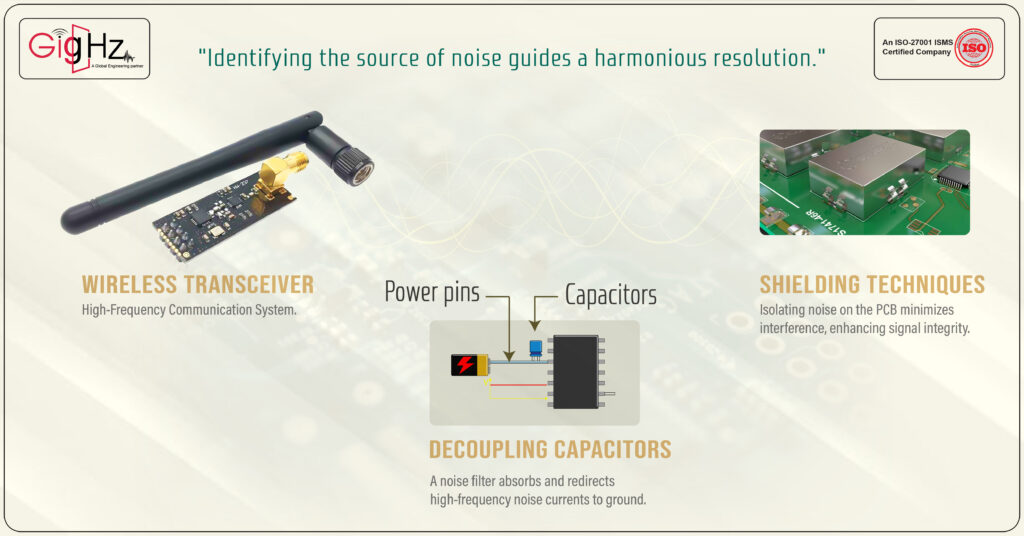
Imagine a scenario where you are designing a PCB for a high-frequency communication system, such as a wireless transceiver. Once you know what type of noise you’re dealing with, you can start identifying the root cause of the problem.
Consider this system operates in a noisy environment with various sources of electromagnetic interference.
In this case, the high-frequency signals generated by the transceiver circuit can propagate as electromagnetic waves, creating electric and magnetic near-fields.
These fields can interfere with other components on the PCB, leading to EMI and potentially degrading the system’s performance.
To address this issue, you strategically place decoupling capacitors near the power pins of the transceiver and other sensitive components. These capacitors act as a “noise filter,” absorbing and redirecting high-frequency noise currents to ground.
As a result, the noise is prevented from spreading to other parts of the PCB, minimizing the chances of interference and improving signal integrity.
Additionally, you incorporate shielding techniques into the design.
By enclosing the transceiver circuitry within a conductive enclosure, you effectively create a shield that blocks external electromagnetic fields from entering the PCB.
This shielding prevents interference from external sources such as nearby electronic devices or radio frequency (RF) signals. It helps maintain the integrity of the communication system, ensuring reliable transmission and reception of data.
Furthermore, you carefully layout and route the traces on the PCB to minimize the coupling between different circuit sections. By employing controlled impedance routing and maintaining sufficient spacing between signal lines, you mitigate capacitive and inductive coupling effects that can introduce noise.
This results in clean, reliable signal paths and reduces the risk of cross-talk or signal degradation.
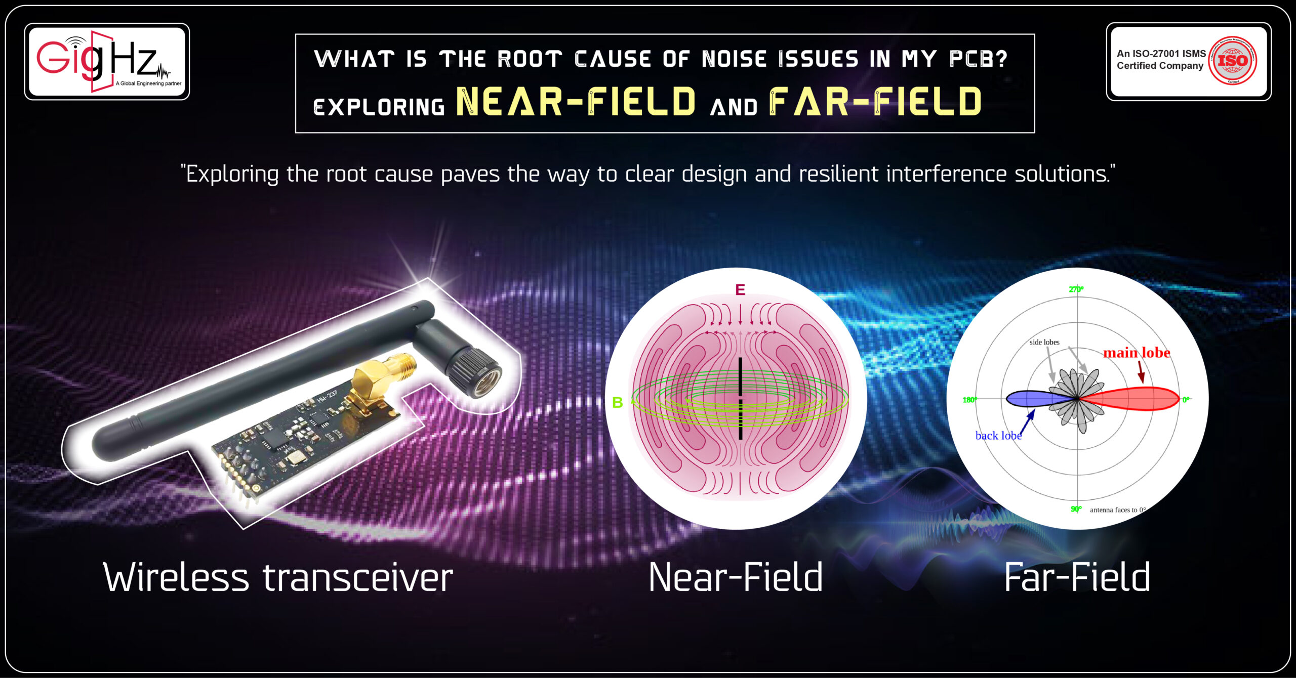
What differentiates the near field from the far field?
You see, the near field and far field are two distinct regions that emerge when we’re talking about electromagnetic radiation.
These regions have their own unique characteristics, and they arise because of how electromagnetic waves behave.
First, let’s talk about the near field.
This region is all about what happens close to a source of radiation, like an antenna or an electronic circuit.
In the near field, the electromagnetic fields are mostly reactive, meaning they don’t behave like typical waves that travel through space. Instead, the electric and magnetic fields in the near field change rapidly in intensity and direction as you move closer to the source. The size of the near-field region is usually just a fraction of the wavelength.
Now, onto the far field.
This region is located much farther away from the radiation source. In the far field, the electromagnetic fields behave more like waves that propagate through space.
You’ll find a well-defined electric field and magnetic field that are perpendicular to each other and perpendicular to the direction of wave propagation. Unlike the near field, the far field extends over long distances and can go on indefinitely.
The transition between the near field and far field occurs at what we call the “Fresnel distance.”
This distance depends on factors like the wavelength of the radiation and the physical dimensions of the source or aperture.
As you move beyond the Fresnel distance from the source, the electromagnetic fields start looking more like regular waves, and the effects of the near field diminish
How Near Field Affects the PCB and How to Mitigate?
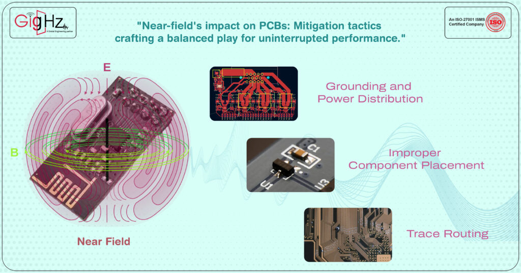
While the transceiver operates in a noisy environment with multiple sources of electromagnetic interference.
Here’s how near-field EMI can affect the performance and how to mitigate it:
Component Placement:
Improper component placement can lead to near-field EMI issues.
For example, if sensitive analog components like the receiver circuitry are positioned too close to high-speed digital components such as the transmitter, electromagnetic coupling can occur.
This coupling can introduce noise and interfere with the receiver’s ability to accurately detect signals. By strategically placing the components at a sufficient distance from each other, you can minimize near-field interference and maintain signal integrity.
Grounding and Power Distribution:
Inadequate grounding and improper power distribution can also contribute to near-field EMI problems.
Ground loops, which occur when there are multiple ground paths with varying impedance, can introduce unwanted noise into the system.
Additionally, voltage fluctuations can disrupt the functionality of the PCB, affecting the wireless transceiver’s performance.
By applying proper grounding techniques, such as star grounding and minimizing ground loop areas, you can mitigate near-field EMI issues and ensure stable power distribution.
Trace Routing:
Poorly routed traces can introduce near-field EMI problems.
For instance, if high-speed signal traces run parallel to sensitive analog traces for an extended distance, capacitive coupling can occur, leading to noise interference.
To mitigate this, you can use controlled impedance routing techniques to match the characteristic impedance of the traces, reducing the chances of near-field coupling.
Additionally, providing sufficient spacing between signal lines can minimize electromagnetic coupling effects.
How Far Field Affects the PCB and How to Mitigate?
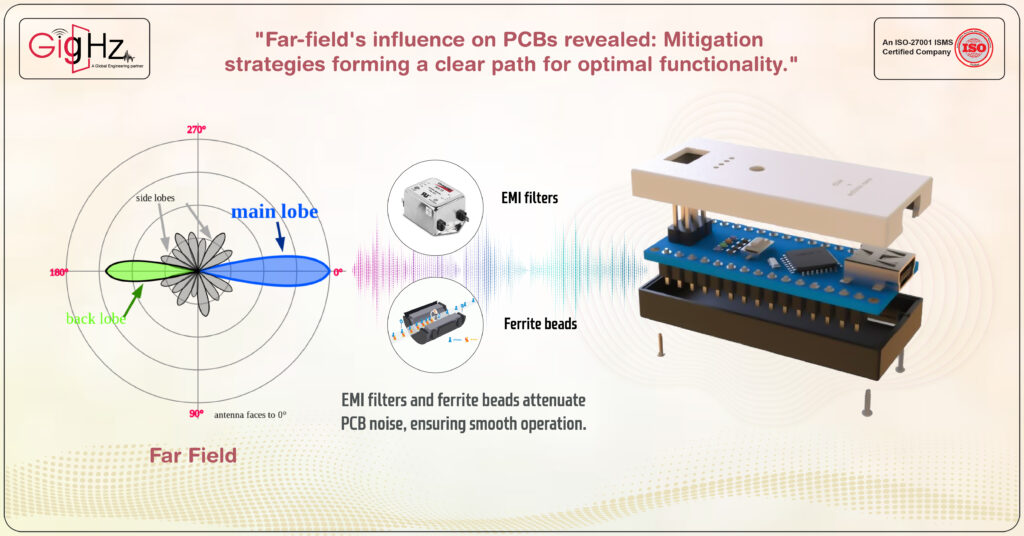
Let’s talk about far-field EMI and how it can be a tricky intruder when it comes to PCBs.
Far-field EMI refers to electromagnetic interference that comes from external sources and impacts the circuitry from a distance.
To combat this, we need to address some key challenges.
One of them is ElectroMagnetic Compatibility (EMC). If we don’t have proper measures in place, external EMI sources can seep into the PCB and cause noise issues.
But fear not!
We can use shielding techniques like metal enclosures or conductive coatings to protect the circuitry from external interference.
By implementing filtering methods such as EMI filters and ferrite beads, we can attenuate the noise entering the PCB and keep things running smoothly.
Another area to focus on is signal integrity.
Inadequate practices, like improper termination or impedance mismatches, can lead to EMI emissions and susceptibility.
We want to ensure that our termination techniques, be it series or parallel terminations, are on point.
Matching impedance is also crucial to improve signal integrity and reduce noise problems.
Don’t forget about grounding techniques! Employing grounding planes or star grounding can help minimize far-field EMI and keep everything in check.
Our Notable Upgrade: Engineering as a Service (EaaS)
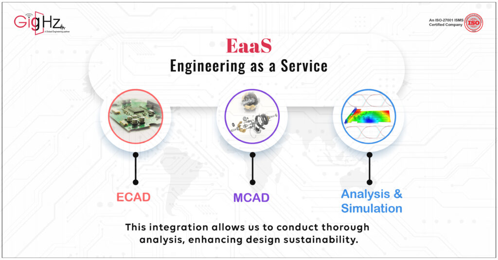
You know, as the need for advanced and integrated engineering solutions keeps soaring, our Engineering as a Service (EaaS) are really stepping up the game.
We’re harnessing the power of ECAD, MCAD, and Analysis & Simulation. This gives us a great position to be frontrunners in this industry.
What’s really cool is that we offer a full package, covering every single step of the engineering process.
And honestly, it’s this kind of approach that’s going to shape the future of our engineering.
It’s exciting stuff!
Why we do?
We challenge our Engineering capabilities with emerging technologies to keep your time and cost in control, thereby transforming product design with human touch quality.
Conclusion
Designing a PCB should consider both near-field and far-field effects that can cause noise issues. Understanding the root cause of these issues is key to putting in place effective solutions.
The use of ground planes, bypass capacitors, signal separation, shielding, and high impedance trace routing can help mitigate noise issues.
Using noise analysis tools can also help you identify noise sources, and control them before they affect your circuit’s effectiveness. With these practices in place, you can ensure that your PCB operates efficiently, meeting all your performance requirements and delivering quality output.
Ready to design a PCB that meets your performance requirements? Reach out to one of our experts today! https://calendly.com/gighz/30min
#Grounding #Shielding #PowerPlaning #Decoupling #SignalRouting #ImpedanceMatching