Our Journey in Designing ECAD for ADAS-Enabled ECUs
Meet the challenging partner of modern cars – the ECU in ADAS! You can call it the ‘smart controller.’ It’s like the boss of all the information from sensors, helping your car stay safe and work better. This little brain acts as a super-smart traffic helper, listening to signals from all over the car. It’s super speedy at understanding things, even quicker than people!

Meet the challenging partner of modern cars – the ECU in ADAS! You can call it the ‘smart controller.’ It’s like the boss of all the information from sensors, helping your car stay safe and work better. This little brain acts as a super-smart traffic helper, listening to signals from all over the car.
Category :
Published Date :
December 12, 2023
Category :
Published Date :
December 12, 2023
Category :
Published Date :
December 12, 2023
Designing this vital part takes time and can be quite complex. A well-designed ECU ensures its features work without any delays.
Since it’s crucial for safe driving, any design issues can have a significant impact. Therefore, great care must be taken during the design process.
Here, we’re sharing our journey of designing an ECAD for ECUs, specifically designed for ADAS applications. We’ll explore the challenges and innovations involved in this essential process.
The Challenges We Faced
This project was a tough phase in our design journey.
We aimed to redo a PCB design, increasing the space between copper areas to 4 mils while keeping components in the same spots.
Since it is a rework design, we have to consider the design aspects under all circumstances and at the same time have to meet the IPC standards.
We also need to improve the impedance control for high-speed signals and increase the width of non-impedance-controlled signals.
This case study outlines our successful approach to achieving these objectives while adhering to Design for Manufacturability (DFM) principles.
Why Space on PCBs Matters?
The trend of shifting towards the miniaturization poses substantial challenges to the design, specifically in hybrid technology that includes high-voltage circuits.
With miniaturization it is possible to merge multiple boards, which also allows the designer to utilize mixed technologies including analog, digital and RF circuits.
PCB line spacing adhering to IPC standards is required to implement precise circuit formation and reducing overall product size.
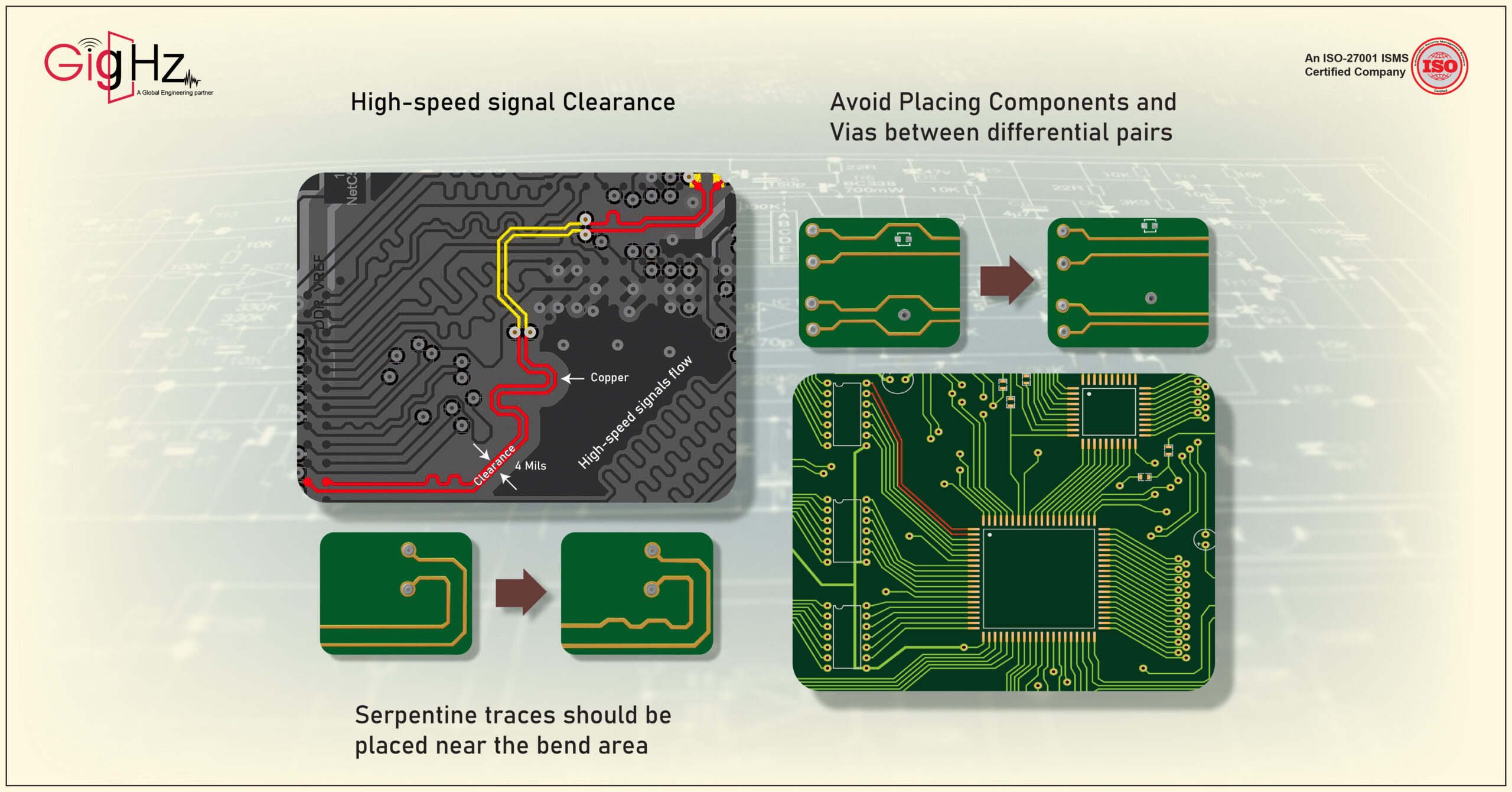
Increasing the Clearance Challenge
In PCB design, the copper-to-copper area distance is known as clearance. If the clearance is less, manufacturing can become challenging.
The project we handled where the client requested an increase in clearance to 4 mils, while the existing PCB had a clearance of less than 3 mils.
Why it is required to increase the clearance?
High speed design needs to have this clearance in order to have suppressed crosstalk in order to ensure a perfect signal integrity.
Also, the clearance was preferred based on the IPC 2221 voltage and spacing standards for preventing ESD between conductors. While preferring the spacing, have to balance both PCB clearance layout and manufacturability.
It is required to check the traces be wide enough to carry sufficient current without becoming too hot.
It is also important to maintain clearance from the bounding surface and through-hole connection points present on the board.
Lower clearance may lead to over-voltage, resulting in instantaneous fault between neighbouring conductive traces.
Non-Impedance-Controlled Signal Width
Our client expected an increase in the width of all non-impedance-controlled signals to 4 mils.
This is the width through which high-speed signals flow. It’s essential to maintain a constant impedance from the start to the end.
However, the existing PCB had widths less than 3 mils.
A targeted impedance on a PCB trace can be attained by varying its width.
Why the impedance needs to be controlled across the line?
If the impedance varies, the voltage also may vary significantly as it is propagated along the trace.
A major issue with boards that don’t have impedance matching is the presence of reflections. So, some of the energy of the signal will reflect toward the driver and the remaining signal will continue onward. When you look at the waveform for this, a pure square wave will not be seen. Rather, a distorted waveform with overshoots and undershoots and some ringing will be observed.
Any unmatched impedances on the PCB will result in some electromagnetic interference (EMI). As a result, the mis-match of the impedance will cause some electromagnetic radiation in that localized area where this transition occurs, and where these reflections appear.
The radiation can couple its energy to neighbouring traces or, affect some susceptible components on the board.
The power is transmitted uniformly across the length of the trace across the PCB only when there is uniform impedance.
Impedance control in PCB design helps products perform better for longer periods of time, improving value and controlled reliability.
Controlled impedance is also essential during transition from a lower ohm to a higher ohm environment where impedance is present. These kinds of transitions can lead to energy reflection in the form of powerful pulses capable of disrupting energy flow.
DFM Principles - Implemented for Our Client
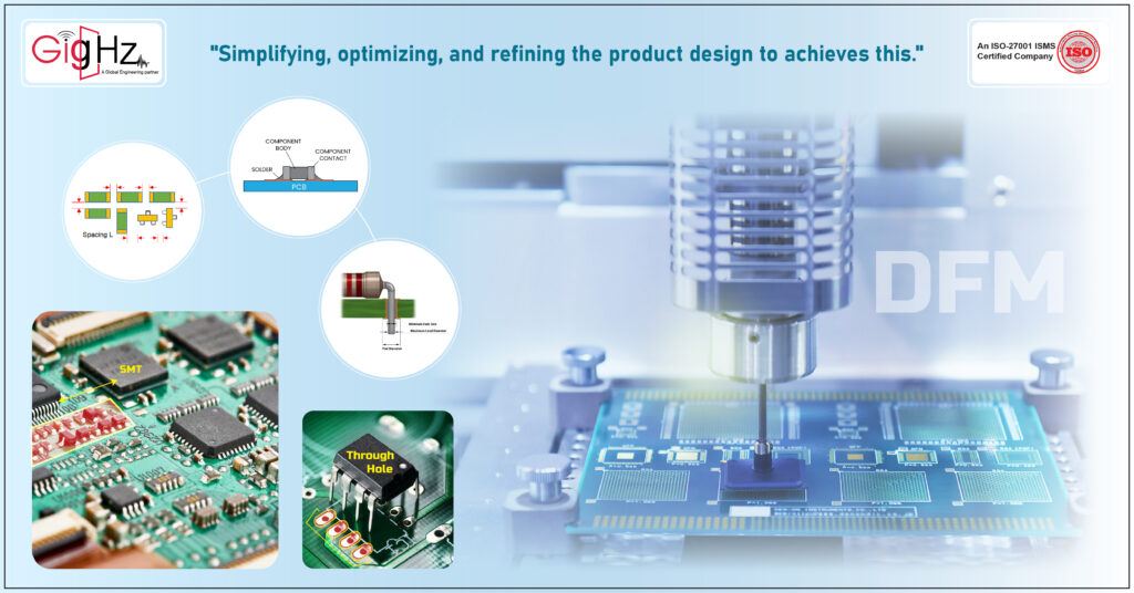
Design for Manufacturing (DFM) is the process of designing parts, components or products for ease of manufacturing with an end goal of making a better product at a lower cost.
This is done by simplifying, optimizing and refining the product design.
Our commitment to Design for Manufacturability (DFM) principles played a pivotal role in the successful execution of the PCB rework project for our client.
We ensured that every aspect of the design adhered to DFM guidelines to optimize the manufacturing process and maintain the highest standards of quality.
Component Placement
Adequate Spacing: We maintained a minimum spacing of at least 40 mils between components, as well as a minimum distance of 100 mils between each component and the edge of the PCB.
This not only facilitates efficient manufacturing but also prevents issues related to component proximity.
Grouping Similar Components
Enhancing Efficiency: By orienting similar components, including passives, in the same direction, we improved the efficiency of the soldering process. This reduced the likelihood of errors during assembly.
Solder Side Considerations
SMT and Through-Hole Segregation: To streamline assembly, we placed all surface mount (SMT) components on one side of the PCB while reserving the top side for through-hole components. This clear separation simplified the manufacturing process and minimized errors.
Minimizing Design Changes
Ripple Effect Mitigation: Recognizing the potential challenges associated with design modifications, we took great care to limit the need for routing adjustments.
This strategy ensured that changes made for manufacturability reduces the risk of encountering signal integrity issues or assembly difficulties.
Our Project Highlights
Our team successfully accomplished the project resulting in a high-quality PCB.
- Precisely increased the clearance from under 3 mils to 4 mils.
- Maintained IPC 2221 voltage and spacing standards
- Succeed by increased the width of all non-impedance-controlled signals to 4 mils from under 3 mils to 4 mils.
- Ensured the PCB design aligned with manufacturability requirements.
- Delivered a seamless rework PCB that met the client’s expectations while improving manufacturability.
Engineering as a Service
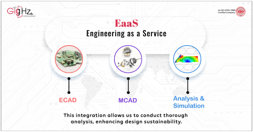
Our strong commitment to the field of electronics involves integrating ECAD (Electronic Computer-Aided Design), MCAD (Mechanical Computer-Aided Design), and Analysis & Simulation to enhance the efficiency of design, production, and operations.
This integration empowers us to perform in-depth analysis, which in turn elevates the sustainability of our designs and yields innovative solutions. The outcome is cost-efficient and high-quality results achieved within an expedited timeline.
Why We Do?

Despite the challenges presented by the ECAD design of ECUs specially made for ADAS applications, we distinguish ourselves through innovative methods and value driven process.
This approach empowers us to achieve a substantial 52% reduction in costs while simultaneously increasing operational efficiency by 25%.
Conclusion
We successfully executed the rework PCB project, meeting the client’s specific requirements for increased clearance and increased width of non-impedance-controlled signal while adhering to DFM principles.
By optimizing the design for manufacturability, we achieved a reliable and manufacturable PCB design that fulfils the client’s expectations.
To experience the EaaS advantage, Book a demo call. https://calendly.com/gighz/30min
Feel free to contact us at with any questions or inquiries. Our team is here to assist you!