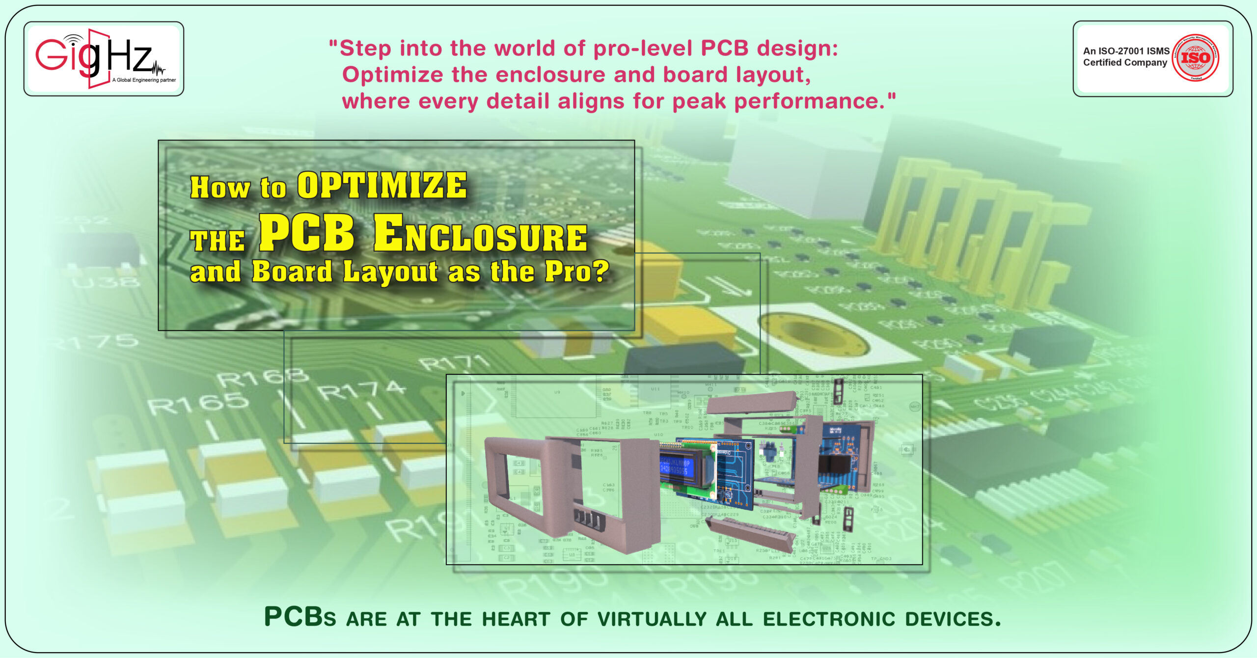
How to optimize the PCB Enclosure and Board Layout as the Pro?
In today’s fast-paced technological era, PCBs are at the heart of virtually all electronic devices, from simple gadgets like calculators to complex systems like supercomputers.
But designing these intricate components is no easy task.
It requires a keen understanding of electrical engineering principles, manufacturing processes, and industry standards.
Category :
Published Date :
February 22, 2024
Category :
Published Date :
February 22, 2024
Category :
Published Date :
February 22, 2024
Aspiring to optimize your PCB enclosure and board layout like a pro?
Great!
You’re about to embark on an exciting journey that combines creativity, precision, and problem-solving.
The process involves meticulous planning, strategic component placement, and careful consideration of thermal management.
But remember, it’s not just about fitting components onto a board.
It’s about ensuring that they work harmoniously within the confines of a specific enclosure, and that they can withstand real-world conditions such as heat, vibration, and electromagnetic interference.
Moreover, it’s also about making the design manufacturable and cost-effective.
This is where Design for Manufacturability (DFM) comes in – a crucial step that ensures your design is not only functional but also easy to manufacture without incurring excessive costs.
So, are you ready to dive deep into the intricacies of professional PCB design optimization?
Let’s get started!
Segregating Modules for Enhanced Performance
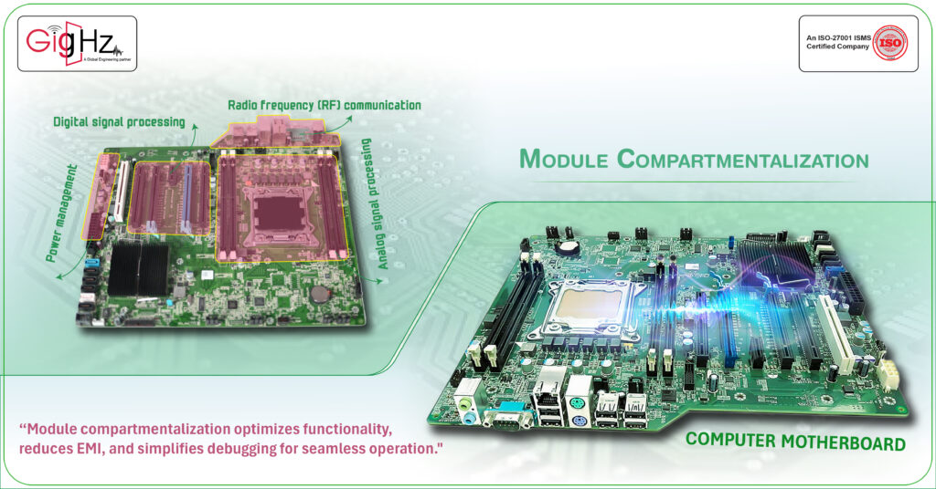
In the context of a Printed Circuit Board (PCB), module Compartmentalization is like dividing the board into specific areas called modules – each serving a unique function such as separate functional units, power management, digital signal processing, analog signal processing, and radio frequency (RF) communication.
The primary technical advantage of this approach is the significant reduction of electromagnetic interference (EMI). EMI can lead to substantial disruptions in electronic devices, with components both generating and being susceptible to it. By isolating different functional sections on a PCB, an ‘electromagnetic boundary’ is created around each module, minimizing EMI and ensuring that one module’s operation does not impact or get affected by others.
With each section focused on a specific function, it becomes possible to optimize each segment’s design. For instance, the power module can be tailored for maximum efficiency, while the RF module can be fine-tuned for optimal signal integrity.
Another benefit of this strategy is the simplification of debugging and testing processes. When an issue arises on a PCB, identifying its source can be challenging. However, by dividing the board into modules, each section can be tested separately, making it easier to identify problems. Once detected, debugging efforts can concentrate on the faulty module without affecting the rest of the board.
A practical example of module compartmentalization can be seen in computer motherboard design. Different sections are allocated to various functions, such as power supply, CPU, memory, and input/output devices. This segregation allows each section to function at its best, contributing to the overall performance of the computer.
The Art of Component Placement
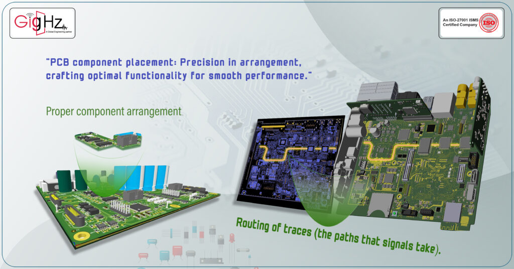
As the part of continuation, in PCB Design, strategic component placement is also vital.
Connectors, which are like gateways for signals, are often placed to facilitate easy connections and minimize potential damage during plugging and unplugging.
Component placement also influences the routing of traces (the paths that signals take). The aim is to keep these paths as short as possible and avoid crossing different signal lines to prevent interference.
Efficient placement ensures better heat distribution and cooling, contributing to the overall performance and longevity of the PCB.
The placement of components on a PCB influences the efficiency of its thermal management system.
When arranged properly, components can dissipate heat more effectively, leading to better performance and longer lifespans for your electronic devices.
Harmonizing Design with ECAD/MCAD Co-design
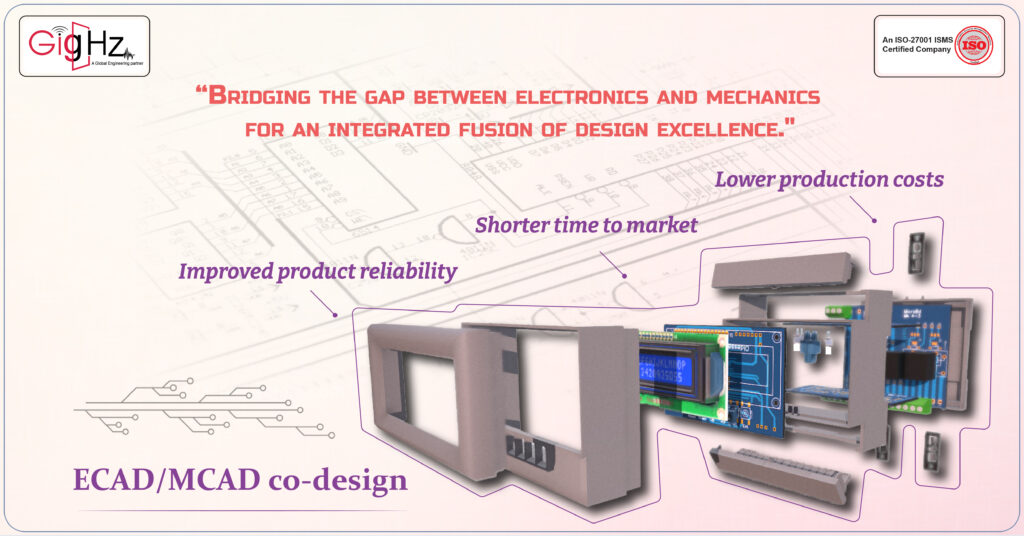
In this the idea we’re examining is ECAD/MCAD co-design. This involves using both Electronic Computer-Aided Design (ECAD) and Mechanical Computer-Aided Design (MCAD) in the creation of a Printed Circuit Board (PCB) and its enclosure.
ECAD is used for designing the electronic layout of the PCB, including component placement, trace routing, and electrical connectivity.
On the other hand, MCAD is used for designing the physical aspects, such as the enclosure that houses the PCB.
When we talk about ECAD/MCAD co-design, it means using these two design approaches together to ensure that both the electronic and mechanical designs align perfectly.
The integration of ECAD and MCAD is crucial because it ensures that the PCB fits seamlessly into its enclosure, with all the connectors and mounts aligned correctly.
This co-design approach decreases the chance of design rework due to mechanical issues, saving both time and resources.
Furthermore, ECAD/MCAD co-design allows for real-time collaboration between electrical and mechanical designers. They can work together concurrently, spotting and solving potential design issues early in the process. This collaborative approach leads to more efficient design workflows and higher-quality end products.
Successful ECAD/MCAD co-design can result in improved product reliability, shorter time to market, and lower production costs. It ensures that the electronic and mechanical aspects of the design are in harmony, resulting in a well-integrated and functional final product.
Navigating EMI & EMC Guidelines for Superior PCB Performance
With the continuation now we’re discussing the concept is Electromagnetic Interference (EMI) and Electromagnetic Compatibility (EMC) guidelines in Printed Circuit Board (PCB) design.
EMI is essentially the noise or interference that can affect the performance of a PCB. EMC, on the other hand, is the ability of the PCB to function properly in its electromagnetic environment without introducing intolerable electromagnetic disturbance to anything in that environment.
Following certain design practices can help reduce EMI and ensure EMC, leading to better-performing PCBs,
These practices could include reducing the length of certain connections to minimize signal degradation and interference. It’s like keeping a conversation short and to the point to avoid misunderstandings. Another strategy is avoiding the creation of unintentional antennas, which can happen when traces or leads act as an antenna and either radiate or pick up interference.
Following EMI and EMC guidelines in PCB design not only helps in creating a better-performing board but also ensures compliance with industrial standards. This can lead to wider acceptance of the final product in the market, making it a win-win situation for both the manufacturers and the end-users.
Perfecting the PCB with Layout Optimization
Lastly, we’re focusing on, is the optimization of layout in Printed Circuit Board (PCB) design.
In PCB design, the layout plays a critical role in how well the board performs. Optimizing the layout involves adjusting and fine-tuning various elements to make sure the PCB operates as efficiently as possible.
This could involve grounding strategies to minimize noise, decoupling to manage power supply fluctuations, and signal routing strategies to maintain signal integrity.
Grounding strategies are used to create a common point of reference for all circuits, minimizing noise. Decoupling, on the other hand, involves placing capacitors between the power supply and ground to smooth out any fluctuations in the power supply.
Signal routing strategies aim to ensure that signals follow the most efficient paths, maintaining their integrity.
The use of simulation tools can come in handy here. These tools allow designers to test and optimize these parameters before the actual manufacturing process begins. It’s like rehearsing a play before the actual performance – you get to spot and fix any issues, resulting in a flawless final act.
Optimizing the layout of a PCB can lead to significant time and cost savings. It can enhance the performance of the board, reduce the likelihood of costly redesigns or modifications, and speed up the time to market.
Our Notable Upgrade: Engineering as a Service (EaaS)
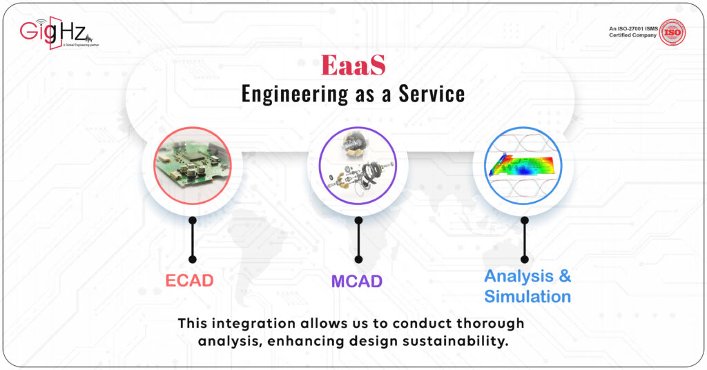
You know, as the need for advanced and integrated engineering solutions keeps soaring, our Engineering as a Service (EaaS) are really stepping up the game.
We’re harnessing the power of ECAD, MCAD, and Analysis & Simulation. This gives us a great position to be frontrunners in this industry.
What’s really cool is that we offer a full package covering every single step of the engineering process.
And honestly, it’s this kind of approach that’s going to shape the future of our engineering.
It’s exciting stuff!
Why we do?
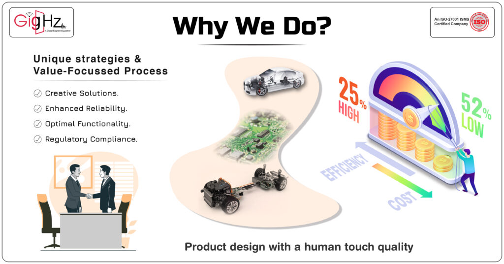
We challenge our Engineering capabilities with emerging technologies to keep your time and cost in control, thereby transforming product design with human touch quality.
Despite these complexities, we distinguish ourselves by implementing unique strategies and a value-focused process.
This differentiated methodology results in a remarkable reduction in costs by 52%, while concurrently enhancing operational efficiency by 25%.
Conclusion
In conclusion, successful ECAD-MCAD collaboration is crucial for efficient and accurate product design. By following best practices such as utilizing co-design approaches, implementing intelligent data management systems, and leveraging automation tools, teams can seamlessly integrate their electrical and mechanical designs.
Asking the right questions, embracing 3D visualization, and enforcing design rules further enhance collaboration. With these tips, businesses can optimize the collaboration process, reduce iterations, and deliver superior products to market.
“Ready to take your design projects to the next level? Discover our Specialities. Visit our Services Page. https://gighz.net/services/
Schedule a Call. Book a free consultation now.https://calendly.com/gighz/30min