Heroic Design & Signal Integrity Analysis in PCB: 7 Concrete Proofs of Excellence in Mirror ISP pcb design Layout
Hey there, fabulous fans of automotive innovation!
Your enthusiasm truly brings joy to my day!
Let’s gear up and dive into the fascinating realm of Advanced Driver Assistance Systems (ADAS) and mirror Image Signal Processor (ISP) layouts.

Hey there, fabulous fans of automotive innovation!
Your enthusiasm truly brings joy to my day!
Let’s gear up and dive into the fascinating realm of Advanced Driver Assistance Systems (ADAS) and mirror Image Signal Processor (ISP) layouts.”
Category :
Published Date :
March 26, 2024
Category :
Published Date :
March 26, 2024
Category :
Published Date :
March 26, 2024
These cutting-edge technologies not only shine with our engineering brilliance but also directly impact our everyday experiences behind the wheel on the road.
I’m thrilled to share with you 7 compelling reasons why these advancements are worth celebrating.
So, let’s rev up our engines and embark on this joyride together!
Our Approach to Addressing the challenges: Signal Integrity Analysis in PCB Design
So, our main gig is all about making sure the PCB layout circuit design fits the bill, meeting those specific requirements while weaving in some signal integrity (si analysis) tricks to make sure those signals flow like a dream.
We’re tackling everything from tricky fine-pitch BGA to the speedy MIPI and LVDS signals, Keeping Separately the Power & HS Signals, Proper type of transmission lines for design decisions, mitigating EMI/EMC and GND bounce effects.
But you know what?
We see these challenges as opportunities to turn things around and come out with even sharper requirements.
It’s all about carefully placing those components, controlling that impedance, and smartly keeping the power and high-speed signals apart, Avoiding Data Corruption, Eliminate Overshoot and undershoot in digital signals.
Our end goal?
A layout that’s not just reliable but also supercharged, giving that ADAS the ultimate performance boost!
Our Methodology in SI Analysis: Putting It into Action for best practices
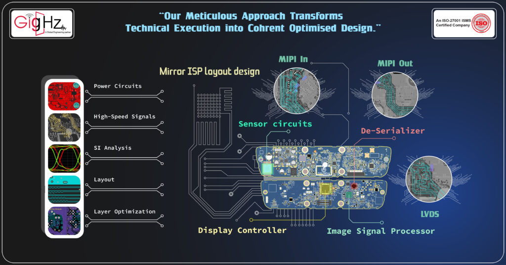
Design of PCB Layout
Initially, the execution of the mirror ISP layout design calls for the seamless integration of various circuits including De-Serializer, Image Signal Processor, Display Controller, and sensor circuits. Emphasizing the incorporation of power circuits and the effective management of high-speed signals is essential to ensure reliable and optimal performance within the ADAS application.
Power Circuits
Now think of the integration of power circuits, including +12V, SEPIC Power (9.5V), Coax Power (8.6V), +3.3V, +5V, +2.0V, +1.8V, +1.5V, and +0.9V, forms the foundational framework for facilitating the operations of our mirror ISP layout.
High-Speed Signals
As we dive deeper into the management of high-speed signals, particularly the MIPI connections from De-Serializer to Video Processor and Video Processor to Display Controller, along with LVDS connections from the Display Controller to the TFT Display connector, ensures the seamless transmission of critical data within the ADAS system.
Signal Integrity Analysis
Now comes the analytical phase, we Leverage advanced tools such as HyperLynx, the signal integrity analysis scrutinizes the layout in depth, identifying operational issues at both interconnect and system levels.
This entails addressing simultaneous switching noise (SSN), return path discontinuities, and ensuring compliance with interface standard requirements such as MIPI CSI.
Analysis Parameters and Results
Still the analysis delves into specific parameters such as voltage levels and interface standard requirements, ultimately aiming to meet the stringent criteria set forth by the video processor and MIPI CSI standards, thereby ensuring the robustness and reliability of the mirror ISP layout.
Layout Recommendations and Implementations
Once the analysis is complete, we delve into the realm of layout recommendations, and implementations lies in addressing specific considerations such as solid GND reference planes, optimized routing, and spacing between GND and signal traces.
This careful optimization contributes significantly to the overall signal integrity and performance of the ADAS system.
Layer Optimization
Then the optimizing layers 6 and 5 for solid GND reference planes, and layer 3 for increased spacing between GND and MIPI signal traces, underscores the precision and attention to detail required in achieving an optimal mirror ISP layout for ADAS applications.
We have transformed the technical execution into a coherent design that links each element of the PCB design process as part of a grand composition, each playing its role harmoniously within the ADAS application.
It’s about continually developing and refining until each piece clicks into place, revealing the complete, functional, and optimized design of our mirror ISP layout.
"Heroic Design & Signal Integrity Analysis in PCB :7 Concrete Proofs of Excellence in Mirror ISP pcb design Layout"
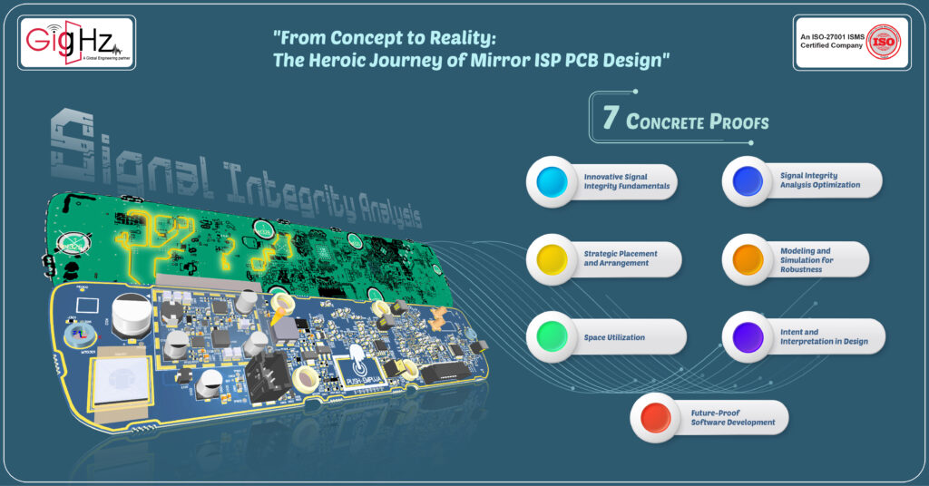
As we delve into the realm of PCB design, signal integrity analysis, and mirror ISP layout, it’s essential to grasp the fundamental aspects that contribute to excellence in this domain.
Let’s embark on a journey to uncover the heroic design and signal integrity analysis of a mirror ISP layout, highlighting seven concrete proofs of its excellence.
- Innovative Signal Integrity Fundamentals: The foundation of a mirror ISP layout lies in understanding the intricate fundamentals of signal integrity within a PCB design. This involves meticulous attention to every aspect, from the choice of components to the fabrication process, ensuring that the signal integrity is upheld at every stage of the layout.
- Strategic Placement and Arrangement: A heroic mirror ISP layout is defined by the strategic placement and arrangement of components, traces, and vias. This includes optimizing signal paths, minimizing interference, and enhancing the overall integrity of the design through thoughtful layout execution.
- Space Utilization: Leveraging space effectively within the PCB layout plays a crucial role in maintaining signal integrity. By exploring layout flags and signatures, designers can capitalize on white space to optimize signal paths and mitigate potential signal integrity issues.
- Signal Integrity Analysis Optimization: An exceptional mirror ISP layout incorporates robust signal integrity analysis This involves in-depth analysis steps that reveal and address potential problems within the layout, ensuring that the integrity of signals is upheld to the highest standard.
- Modeling and Simulation for Robustness: The heroic nature of a mirror ISP layout is further exemplified thorough modeling and simulation. By developing and executing models designed to support assessment of signal integrity, designers can ensure the robustness and effectiveness of the layout.
- Intent and Interpretation in Design: Understanding the intent and interpretation behind every design decision is pivotal in achieving excellence in mirror ISP layout. Intentional design choices and interpretations play a key role in upholding the integrity of signals and ensuring a cohesive layout structure.
- Future-Proof Software Development: Looking ahead, future-proof software development is essential for maintaining excellence in mirror ISP layout. Analyzing and demonstrating future software development savings, alongside optimizing power efficiency, contributes to the longevity and adaptability of the designed layout.
By unravelling these seven key elements, we gain a deeper understanding of what constitutes a heroic design and signal integrity analysis and integrity simulations in a mirror ISP layout.
These elements collectively form the bedrock of excellence, setting the stage for superior performance, reliability, and innovation within the realm of PCB design and signal integrity.
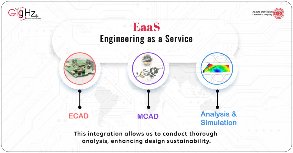
"Our Memorable Advancement": Engineering as a Service(EaaS)
Definitely!
- As complex engineering challenges become more prevalent, our Engineering as a Service (EaaS) offering is truly elevating its presence.
- We are leveraging the combined strengths of ECAD, MCAD, and Analysis & Simulation, which establishes us as leaders in the field.
- What’s particularly exciting is that we provide a comprehensive solution, encompassing the entire engineering workflow.
- It’s genuinely exhilarating!
Why we Do?
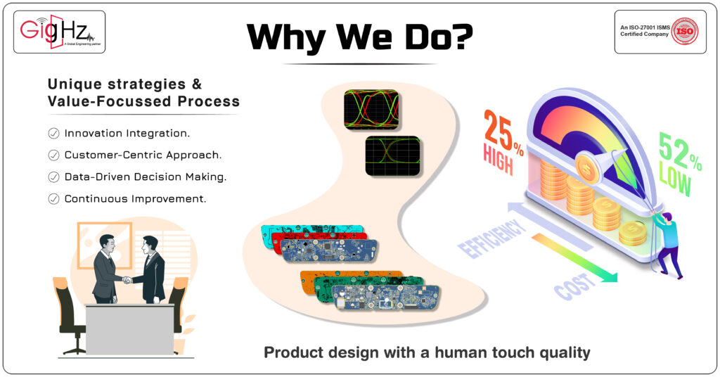
Our drive originates from the complexity with Signal Integrity Analysis reaching into the Automotive Industry.
Despite these intricacies, we set ourselves apart by deploying distinctive strategies and a value-centric approach.
This unique methodology leads to an impressive 52% cost reduction, coupled with a 25% improvement in operational efficiency.
Conclusion
We have demonstrated unwavering dedication to delivering excellence and our robust technical proficiency by offering a suite of recommendations aimed at enhancing signal integrity in your board.
These suggestions have been adeptly integrated into the advanced pcb layout design, elevating its performance significantly.
Our engagement with the client goes beyond mere technicalities; it involves enriching pcb signal design and routing performance through a fusion of our in-depth expertise and a comprehensive grasp of the client’s needs.
Uncover Our unique Expertise. Explore Our Services Today! https://gighz.net/services/
Our commitment to exemplary Analysis services evidences our competence and reliability in securing remarkable outcomes.
Claim Your Spot for a One-on-One Call! https://calendly.com/gighz/30min