From A to Z: Unpacking Signal Crosstalk in Electronic Board Design
Hello to all the tech wizards out there!
Today, we’re going to delve into a topic that might seem a bit complex at first but trust me, by the end of this blog, you’ll grasp it with ease.
We’re talking about signal crosstalk in electronic board layouts, a common yet crucial concept in the world of PCB (Printed Circuit Board) design.
Imagine You’re on a road trip, relying on your smartphone for navigation, entertainment, and communication.
Suddenly, your battery starts to drain rapidly.
Frustration sets in as you desperately search for a power source.
But what if there was a way to charge your device rapidly, allowing you to get back on track without any interruptions? USB PD is the solution you’ve been waiting for!
Category :
Published Date :
December 28, 2023
Category :
Published Date :
December 28, 2023
Category :
Published Date :
December 28, 2023
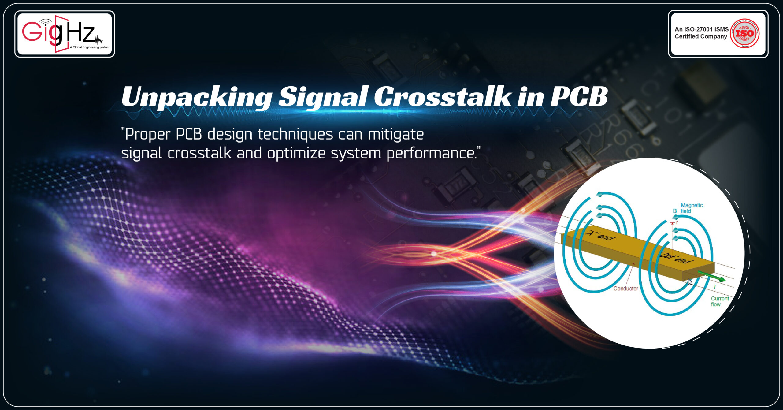
Firstly, let’s understand the science behind crosstalk.
When electrical signals travel through conductive paths in a PCB, they create an electromagnetic field around them. If another conductive path is too close to the first one, this electromagnetic field can induce a voltage or current in the second path. This undesired signal, or ‘noise’, is what we call crosstalk.
This disruption can lead to signal distortion, noise, timing errors, and in severe cases, complete system failure.
In today’s digital age, PCBs are at the core of almost every electronic device, and the issue of crosstalk is becoming increasingly important to designers and engineers.
Crosstalk is not a random occurrence and can be calculated.
To do so, you need to consider factors like signal rise time, trace spacing, trace length, and the dielectric constant of the PCB material.
In this blog post, we will take a deep dive into crosstalk basics to help you understand what it is, how it affects PCBs, and what you can do to mitigate its effects
Understanding Signal Crosstalk
Signal crosstalk is an unwanted effect that occurs when an electrical signal interferes with another, causing disruption or misinterpretation of the signal data.
This typically happens in printed circuit boards (PCBs) where multiple traces are close to each other, resulting in electromagnetic fields that can interfere with each other.
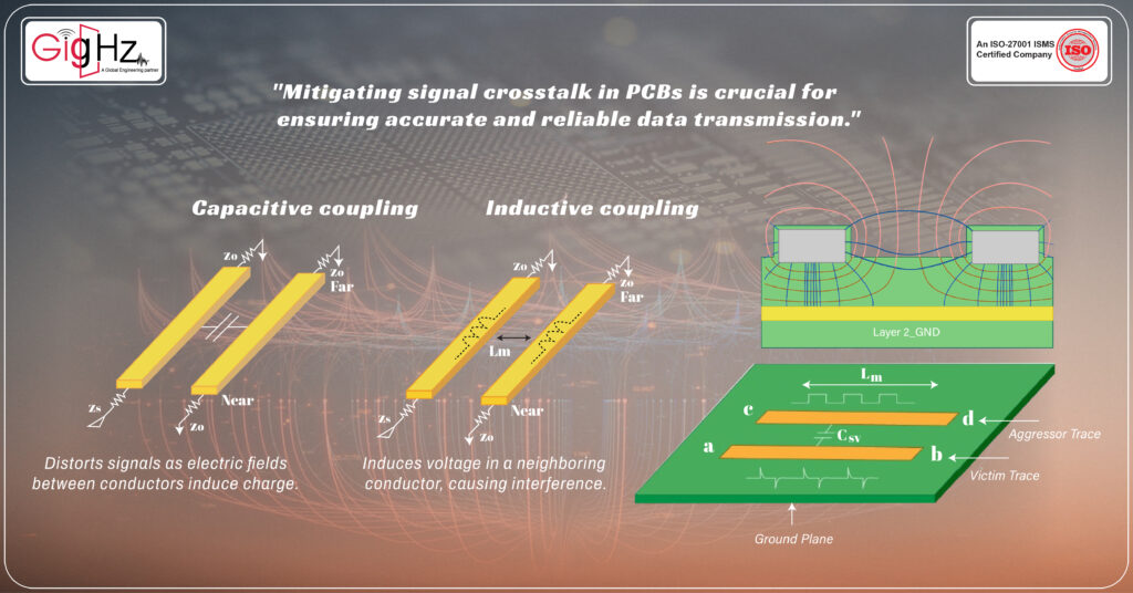
Crosstalk is primarily caused by two mechanisms: capacitive coupling and inductive coupling. Capacitive coupling takes place when the electric field of one conductor affects another nearby conductor, creating an electric charge that can distort the original signal.
Inductive coupling, on the other hand, occurs when the magnetic field from one conductor induces a voltage in a neighbouring conductor, leading to interference.
The frequency of the signals passing through these conductors also has a significant impact on crosstalk. Higher frequencies are more susceptible to crosstalk due to their shorter wavelengths.
Thus, designers working on high-speed designs need to be particularly mindful of mitigating crosstalk.
The spacing between traces plays a crucial role in crosstalk. Traces that are closer together have higher chances of interference as their electromagnetic fields are more likely to overlap.
Therefore, increasing the distance between traces can help in reducing crosstalk.
The material of the PCB can also affect crosstalk. Materials with higher dielectric constants can help reduce the likelihood of crosstalk, as they can better insulate the conductors and prevent the interference of electromagnetic fields.
Effects of Crosstalk on PCBs

Crosstalk can have numerous undesirable effects on Printed Circuit Boards (PCBs), there are two types of crosstalk: near-end crosstalk (NEXT) and far-end crosstalk (FEXT). NEXT occurs when the crosstalk happens close to the source of the signal, while FEXT takes place towards the end of the signal’s path.
NEXT is the more common and problematic type of crosstalk, as it occurs in high-frequency circuits where signals travel fast, including signal distortion, signal attenuation, cross-signal coupling, and signal reflections.
Signal distortion, which involves changes to a signal’s frequency or waveform during transmission, can lead to errors at the receiving end. This distortion can be attributed to several factors such as impedance mismatch, temperature variations or power supply noise, all of which can compromise the overall system performance.
Signal attenuation refers to the reduction in signal strength during its journey through the PCB and is caused by various factors including the resistance and capacitance of the PCB material, the length and width of the traces, and the frequency of the signal. High-frequency signals are particularly susceptible to attenuation.
Cross-signal coupling (crosstalk) occurs when signals on adjacent traces interact with each other – a common occurrence in high-density PCB designs where traces are closely packed. This interaction can lead to unwanted signal interference, causing data errors and system malfunctions.
Finally, signal reflections occur when signals bounce back along a trace due to incorrect termination, leading to signal delay and phase distortion, which can affect the timing and synchronization of the system. To reduce signal reflections, proper termination techniques such as using matching impedance should be employed.
Maintaining signal integrity and ensuring reliable PCB performance requires understanding and mitigating the effects of crosstalk, which involves careful PCB layout design, appropriate component selection, and the use of proper termination techniques
Mitigating Crosstalk
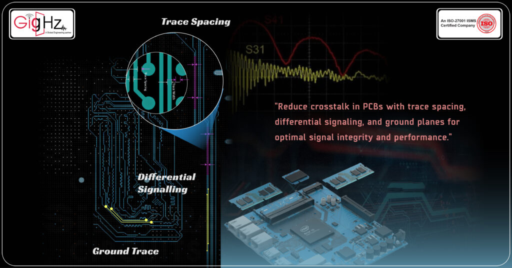
Designers can significantly reduce crosstalk in Printed Circuit Boards (PCBs) by implementing a range of techniques, including trace spacing, differential signalling, and the use of ground planes.
Trace spacing, which is the distance between adjacent traces on a PCB, plays a crucial role in crosstalk mitigation.
By increasing this distance, particularly between critical signals, the effects of crosstalk can be greatly minimized. This is because the electromagnetic fields generated by one trace are less likely to affect another if they’re further apart. However, due to size constraints in high-density PCB designs, this method isn’t always feasible.
Another effective technique for reducing crosstalk is differential signalling.
This involves sending two complementary signals on adjacent traces but in opposite phase. This means that any noise picked up by both traces will be common-mode noise, which is cancelled out at the receiver end. As a result, differential signalling is highly resistant to crosstalk and other forms of electromagnetic interference.
The use of ground planes is another popular method for mitigating crosstalk.
A ground plane is a large area of copper that runs through the entire PCB. It acts as an electrical shield, blocking electromagnetic fields from reaching sensitive traces. Ground planes also provide a return path for signals, which can help reduce loop areas and thus decrease electromagnetic radiation.
In addition to these methods, certain routing techniques can also help reduce crosstalk.
For example, routing traces at right angles on adjacent layers can minimize the overlapping of electromagnetic fields and thus reduce crosstalk. Furthermore, keeping traces as short as possible can also help minimize potential interference.
Understanding and implementing these techniques can greatly aid designers in mitigating crosstalk, thereby enhancing signal integrity and overall PCB performance.
Simulations and Validation
Simulation tools are software solutions that allow designers to create a virtual model of their PCB design. They can then predict how the board will behave under different scenarios, including the levels of crosstalk that may occur. This is done by analyzing the electromagnetic fields generated by signals as they pass through the traces.
The tool can simulate various factors such as trace spacing, trace length, and signal frequency, among others. This allows the designer to see where potential issues may arise and make adjustments as necessary.
For instance, if the simulation shows high crosstalk in a particular area, the designer might decide to increase trace spacing or use differential signalling in that part of the design. By using these tools, designers can optimize their design for maximum signal integrity before the board is physically produced.
A network analyzer might be used to measure the S-parameters of the PCB, which can provide information about transmission and reflection coefficients.
If the measured performance matches the predictions made during the simulation phase, this confirms that the design is sound and the mitigation techniques have worked as intended
Why We Do?

We challenge our Engineering capabilities with emerging technologies to keep your time and cost in control, thereby transforming product design with human touch quality.
Conclusion
Cross-talk is a reality of the PCB design process, and it should never be overlooked.
Having an expert on board who can tackle crosstalk issues and use effective mitigation techniques is essential for building reliable and high-performance boards.
As we have decades of experience in dealing with crosstalk issues and can provide solutions to any problems you may be facing.
So don’t wait any longer – get in touch with us now and make sure your circuit boards become the best possible version they can be! info@gighz.net