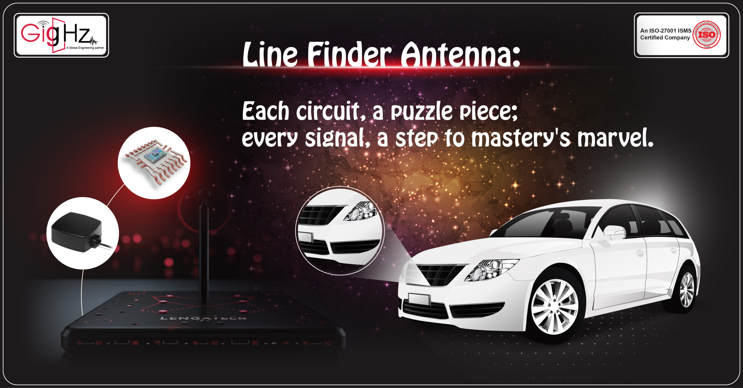
Exploring the Line Finder Antenna-Magnetic Sensor Technology
Introducing the Line Finder Antenna of Magnetic Sensor, an innovative system crafted for detecting magnetic signals interactively. Metal object detection in cars employs magnetic sensors, strategically placed in areas like the front and rear bumpers. These sensors detect alterations in the magnetic field induced by nearby metal objects.
Here at GigHz, we’re in the business of turning “impossible” into “done.”
We thrive on tackling complex challenges and transforming them into innovative solutions.
Recently, we had the chance to flex our problem-solving muscles when a client came to us with a tricky situation involving a hosted payload sensor data collection in their spacecraft.
Category :
Published Date :
February 6, 2024
Category :
Published Date :
February 6, 2024
Category :
Published Date :
February 6, 2024
Primarily utilized in parking assistance systems, they play a crucial role in enhancing safety. When a metal object, such as another vehicle or obstacle, is sensed, the system promptly alerts the driver through beeps or visual signals.
This technology significantly contributes to safer parking by assisting drivers in avoiding collisions, particularly in confined spaces where visibility may be limited.
Join us in exploring the intricate process behind its creation, from circuit design to prototype board development.
Witness how we select the optimal components, integrate advanced signal processing capabilities, and meticulously calibrate and test for flawless precision.
Step into the world of magnetic signal identification and embark on a journey toward revolutionary applications and solutions in magnetic signal detection.
Herewith, sharing you, our project journey of magnetic sensor from circuit design to prototype board design.
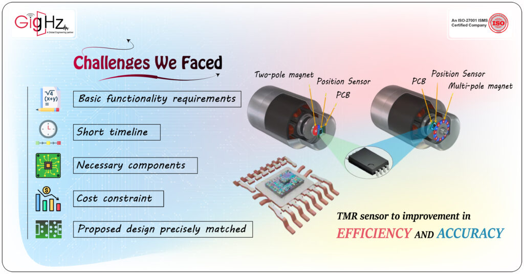
The Challenges We Faced
While striving to upgrade an underperforming existing design, we encountered multifaceted challenges in our quest for enhanced accuracy and performance.
Amidst the upgrade process, several challenges were emerged throughout our project work flow.
Listing out the challenges below:
The existing design’s inability to meet the desired accuracy required a series of updates and modifications.
In the existing design, the mechanism totally relied on inductor coil where we need to replace it with TMR sensor to get a notable improvement in efficiency and accuracy.
However, the absence of basic functionality for its specific parameters posed a significant challenge. Sourcing accurate formulas to define these parameters became a critical necessity in the modification process.
Complicating matters further was the pressing issue of a short timeline. The urgency for swift progress added immense pressure to source formulas, conduct evaluations, and implement modifications within a tight schedule.
Moreover, ensuring the availability of necessary components within this limited timeframe proved to be another intricate challenge. The successful execution of the proposed design was heavily dependent on securing these components promptly.
Adding to the complexity was the stringent cost constraints. It was imperative that the expenses for the proposed design did not surpass ten times the cost of the existing design. This requirement demanded a delicate balance between cost-effectiveness and achieving the desired performance enhancements.
A paramount challenge was to ensure that the values of parameters in the proposed design precisely matched those of the existing design parameters such as Design sensitivity, Noise Performance, Frequency Response, Maximum Magnetic Field before saturation.
This precise alignment while improving accuracy and performance became a pivotal yet intricate task in the modification process.
The Project Work Flow
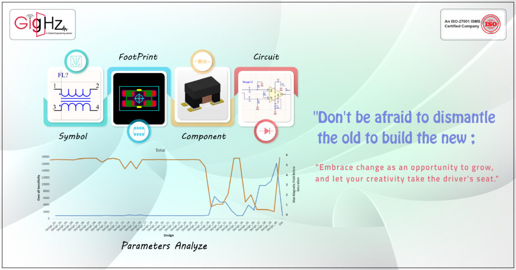
The task at hand involved an in-depth exploration, identification, and documentation of formulas, calculations, and parameter values inherent in existing design configurations. This meticulous process aimed to extract crucial data essential for the modifications.
Simultaneously, sourcing and compiling a comprehensive list of alternative components for the proposed design aligned with specific requirements formed a critical phase. This step necessitated finding suitable replacements within the given constraints and specifications.
The subsequent phase involved the creation of a new model circuit using parameter values either matching or surpassing the performance benchmarks set by the existing version. This step demanded precision to enhance accuracy and overall performance.
Following this, a diverse array of design combinations was generated by integrating components and conducting exhaustive analyses and calculations. Each combination’s parameters and Bill of Materials (BOM) cost were meticulously documented to enable comprehensive comparison.
Thorough analysis of all parameters was conducted to discern the most promising combinations from the extensive list, aligning with the specified criteria. This critical evaluation sought to identify combinations that excelled across all defined parameters.
To conclude, the development of Symbol and Footprint libraries for all components within the selected best combinations marked the final step. This comprehensive approach aimed to ensure seamless integration and efficient utilization of components within the chosen designs.
Schematic Creation
Designing a schematic diagram for the best combinations involved implementing a variant concept to facilitate testing on a single prototype-level board. This process required for blending the chosen combinations into a cohesive schematic layout, ensuring compatibility and feasibility for integration on a singular board.
The schematic diagram’s creation encompassed meticulous planning and arrangement, mapping out the interconnections and placements of components from the selected combinations. It aimed to streamline the prototype-level testing by consolidating various design variants onto a single board for efficient assessment.
Implementing the variant concept involved a strategic approach to accommodate multiple design configurations within a unified schematic layout. This step demanded careful consideration of connectivity, compatibility, and optimization to ensure accurate representation and efficient testing of the diverse combinations.
Ultimately, the schematic diagram served as a blueprint for integrating and evaluating the multiple design variants on a single prototype-level board. Its comprehensive design allowed for streamlined testing, enabling thorough assessments of the chosen combinations’ performance and functionality within a unified testing environment.
PCB Layout
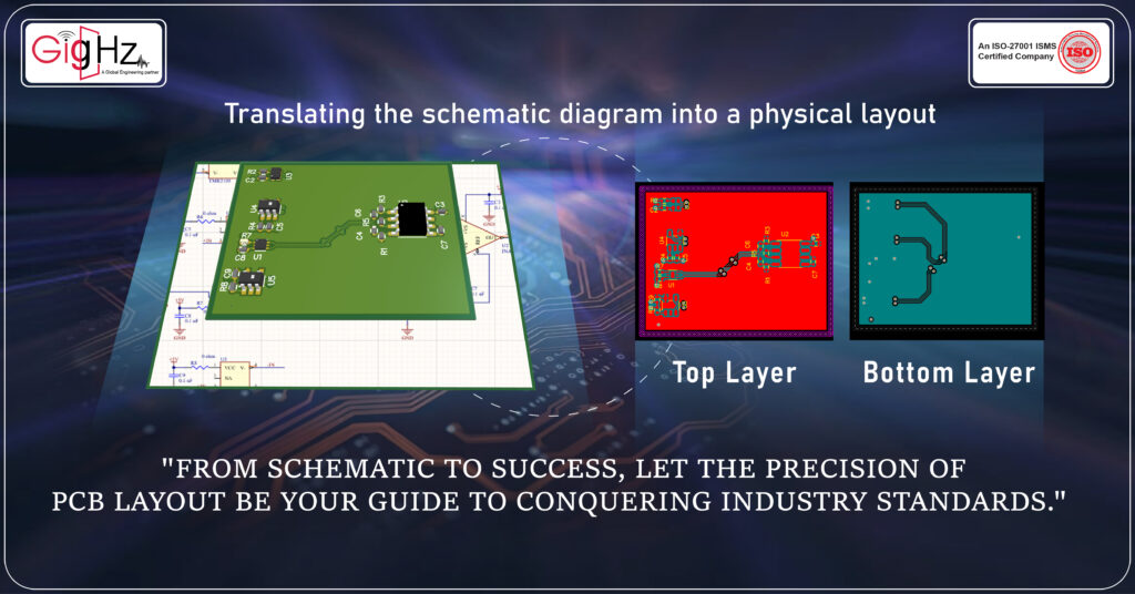
The development of the PCB layout aligned closely with the schematic designed earlier, meeting the precise standards outlined by the client. This phase involved translating the schematic diagram into a physical layout while adhering meticulously to the client’s specified standards and industry best practices.
The deliverables for the PCB design outputs were meticulously prepared, ensuring compliance with stringent industry standards. These outputs encompassed a comprehensive set of documents, including Gerber files, fabrication drawings, assembly drawings, and Bill of Materials (BOM), all meticulously compiled and organized according to industry norms.
The PCB layout aimed for optimal functionality and manufacturability, considering factors like component placement, signal integrity, power distribution, and thermal management. It was crucial to meet the client’s specified standards while ensuring that the design complied with industry regulations and guidelines.
Moreover, the PCB design outputs were prepared with utmost precision and detail, providing all necessary information and instructions required for manufacturing and assembly. The comprehensive nature of these deliverables aimed to facilitate seamless production and ensure that the final PCB met the client’s expectations and industry benchmarks.
Our Notable Upgrade
In the existing PCB design, when a change in magnetic field occurs, the inductor coil will produce an induced current.
On connecting this to the amplifier circuit in Transimpedance formation (Current to voltage converter circuit), the induced current is then converted into voltage and amplified and analysed the sensitivity of the circuit as 875.954 (mV/μT).
Then, the amplified voltage is transmitted out of this board through a connector for metal object detection application.
In the proposed PCB design, TMR sensor (Tunnel Magneto-Resistance) senses the magnetic field, depending upon magnetic field change, sensor produce the voltage, with connecting this to the Instrumentation amplifier circuit, to amplify the voltage signal and improved the sensitivity of the circuit to 1084.5(mV/μT).
Then, the amplified voltage is transmitted out of this board through a connector for the existing application.
Why Proposed Design?
TMR sensors can be highly sensitive to magnetic fields, allowing for precise and accurate measurements compare to the inductor coil in the existing design.
Why we do?
We’re driven by the complexities of the Line Finder Antenna’s magnetic sensor, spanning from circuit to prototype board design. Despite these challenges, we stand out by employing innovative methodologies and a value-centered process.
Through this distinct approach, we achieve a notable 52% cost reduction while simultaneously boosting operational efficiency by 25%.
Conclusion
In our journey from circuit design to prototype board creation, we showcased unwavering dedication and technical expertise, aligning precisely with our client’s needs. Our collaboration is a fusion of proficiency, personalized service, and technical excellence.
Our commitment is evident in the delivery of top-tier circuit designs to prototype PCB layouts. Not only do these efforts reduce costs, but they also emphasize our reliability in consistently achieving exceptional results. Our focus remains on quality and adherence to timelines, setting benchmarks for excellence.
Join us in unlocking innovation and precision for your projects.
Experience our commitment to delivering exceptional circuit designs and prototype PCB layouts tailored precisely to your needs.
Schedule a call. Book a Free Consultation Now.https://calendly.com/gighz/30min
Let’s shape excellence together!
To discover our specialties, visit our website by clicking here. www.gighz.net