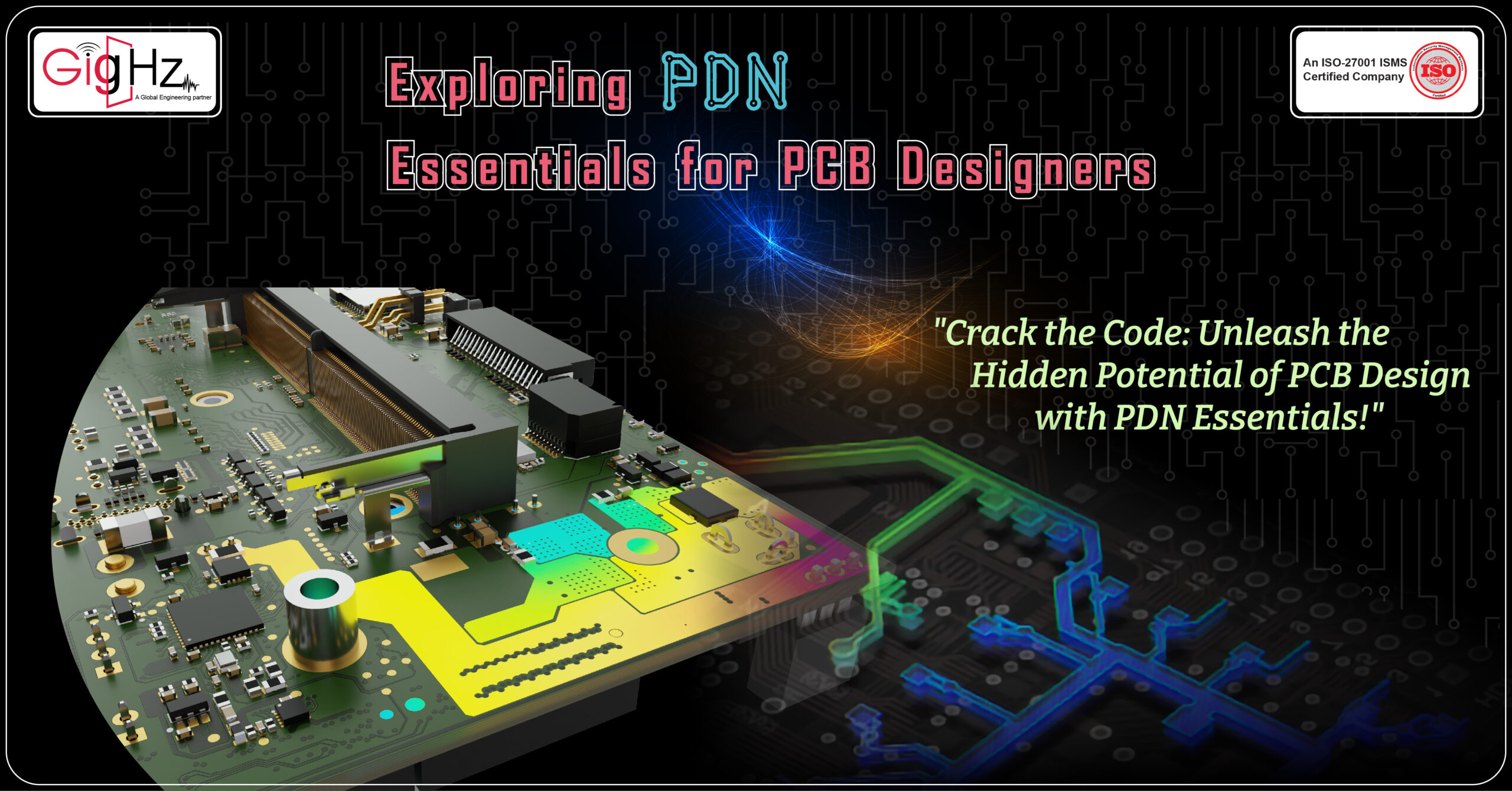
Exploring PDN Essentials for PCB Designers
In today’s technologically advanced world, electronic devices have become an integral part of our daily lives. From smartphones to smart home devices, these gadgets rely on printed circuit boards (PCBs) to function efficiently. At the heart of every PCB lies the power distribution network (PDN), responsible for delivering clean and stable power to all components
In today’s technologically advanced world, electronic devices have become an integral part of our daily lives. From smartphones to smart home devices, these gadgets rely on printed circuit boards (PCBs) to function efficiently. At the heart of every PCB lies the power distribution network (PDN), responsible for delivering clean and stable power to all components.
Category :
Published Date :
January 11, 2024
Category :
Published Date :
January 11, 2024
Category :
Published Date :
January 11, 2024
A well-designed PDN is essential for maintaining the integrity of signals, reducing noise interference, and preventing voltage drop issues.
It ensures that each component on the PCB receives the required power without compromising performance. Therefore, having a solid understanding of PDN essentials is crucial for PCB designers.
Throughout this guide, we will cover the key components and considerations involved in PDN design.
We will start by explaining the basics of PDN, including its purpose and the role of various components such as power planes, power rails, decoupling capacitors, and ground planes.
We will also discuss the importance of analyzing power requirements and estimating power budgets for effective PDN design.
One of the significant factors to consider in PDN design is target impedance. Achieving the desired impedance helps control power fluctuations and minimizes voltage drops, ensuring stable power distribution.
We will delve into the concept of target impedance and discuss techniques for achieving it in your PCB design.
Additionally, we will explore the use of decoupling capacitors in PDN design. These capacitors act as energy reservoirs, mitigating noise and voltage fluctuations.
Let’s get started,
Understanding the Basics of PDN
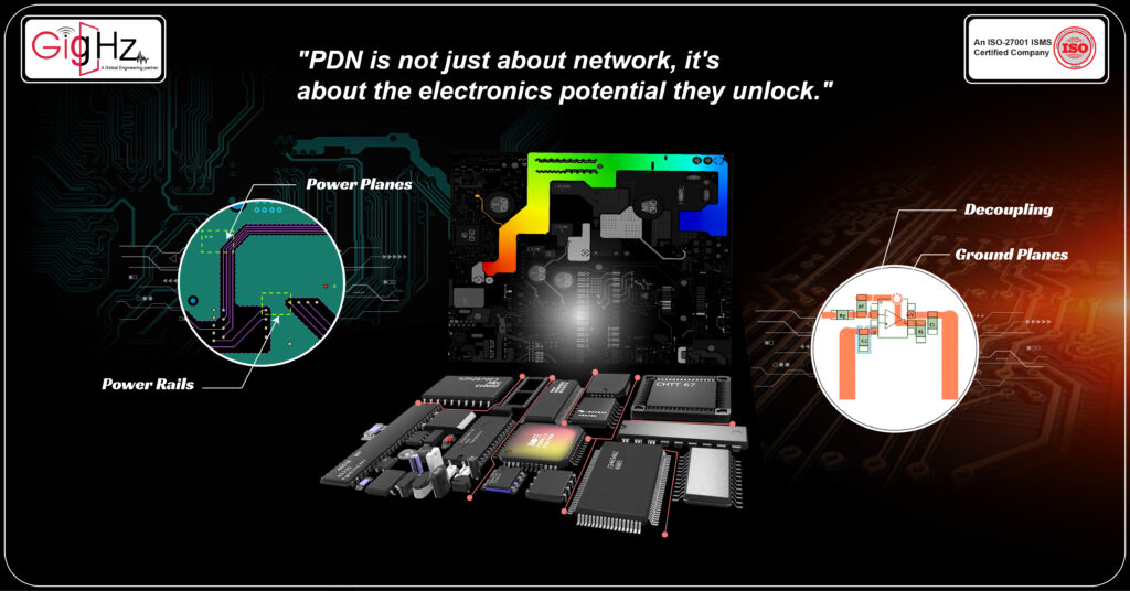
When designing a PCB, it is crucial to have a well-designed power distribution network (PDN) that effectively delivers power to various components. To gain a deeper understanding of PDN basics, let’s break down its key components and their roles.
Power planes are conductive layers in the PCB that act as a central hub for distributing power throughout the circuit. They provide low impedance paths for power delivery and help minimize voltage drops. Typically, a PCB has multiple power planes, such as VCC and GND planes, which supply power and act as return paths for the current.
Power rails are conductive traces that connect components to the power planes. These traces carry the power from the power source to the different parts of the circuit. Proper routing and sizing of power rails are crucial to ensure efficient power distribution and prevent excessive voltage drops.
Decoupling capacitors are strategically placed near individual components or groups of components to provide local energy reservoirs. They work by storing electrical charge and releasing it when needed, reducing noise and voltage fluctuations. Decoupling capacitors help stabilize the power supply and improve overall circuit performance.
Ground planes act as a reference point for the circuit’s voltages. They provide a low impedance return path for the current flowing through the power planes and power rails. Ground planes also help reduce electromagnetic interference (EMI) and provide shielding from external noise sources.
Considerations of PDN Design

When designing the Power Delivery Network (PDN) for a PCB, several considerations must be taken into account.
First and foremost, it is crucial to analyze the power requirements and estimate the power budget for the board. This involves understanding the voltage levels and current demands of the components, as well as any special power needs, they may have. By carefully considering these factors, designers can ensure that the PDN can meet the power demands of the entire system.
Another important concept in PDN design is target impedance. Target impedance refers to the desired characteristic impedance of the power delivery network. Achieving the target impedance is critical as it helps control power fluctuations and minimize voltage drops across the PCB. By carefully controlling the impedance, designers can maintain signal integrity and reduce the risk of electromagnetic interference.
Decoupling capacitors play a vital role in PDN design. Acting as local energy reservoirs, these capacitors provide a stable source of power to high-speed and noise-sensitive components.
However, proper placement and selection of decoupling capacitors are crucial to effectively minimize noise and voltage fluctuations. Designers must consider factors such as capacitor values and placement near power pins to maximize decoupling effectiveness.
In addition, thermal considerations are essential for PDN design.
Overheating can lead to component failures and decreased reliability. To mitigate this, designers should implement proper thermal management techniques such as thermal vias, heatsinks, or copper pours to dissipate heat from high-power components. Adequate spacing between power planes and sensitive components also helps prevent thermal hotspots that could affect signal integrity. By carefully addressing thermal concerns, designers can ensure optimal performance and reliability
Techniques for Optimising PDN Performance
Power integrity analysis using simulation tools is essential to analyze and validate the behavior of the PDN. By identifying issues such as excessive voltage drops, high impedance areas, and power delivery inefficiencies, you can fine-tune the PDN design for improved signal integrity and power delivery.
Controlling power plane impedance is another effective technique. By carefully designing the PCB stackup and determining copper thickness, you can control the impedance of the power planes. This helps ensure efficient power transfer and reduces losses in the PDN, leading to improved overall performance.
Reducing inductance is a crucial consideration in PDN design. Inductance can cause voltage drops and affect high-frequency signal integrity. Techniques such as increasing the number of vias and keeping return paths close to signal paths can help minimize inductance, resulting in enhanced performance.
Optimizing decoupling capacitor placement is also important. Placing decoupling capacitors as close as possible to the power pins of high-speed and noise-sensitive components, minimizing loop area, and using a combination of capacitor values can improve decoupling effectiveness and noise suppression.
Finally, employing optimal routing techniques contributes to PDN performance optimization. Utilizing wider traces or power planes for high-current paths, minimizing trace lengths, and reducing the use of vias can help minimize impedance variations and improve power delivery efficiency.
Challenges and Solutions in PDN Design

High-speed signalling introduces complexities such as simultaneous switching noise (SSN) and signal degradation.
To mitigate these challenges, it is important to separate signal and power planes, employ controlled impedance routing, and strategically place decoupling capacitors.
EMI/EMC concerns are also critical in PDN design, as unwanted noise and emissions can impact circuit performance and regulatory compliance. To address these concerns, proper grounding techniques, shielding, and thoughtful component placement should be implemented.
Thermal management is another key aspect of PDN design, particularly in power-intensive applications. Adequate thermal relief, efficient heat sinking methods, and the use of thermal vias in strategic locations help dissipate heat and prevent thermal issues that can degrade PDN performance.
Additionally, the PCB stackup design plays a significant role in PDN performance. Factors such as layer count, materials, and copper thickness need to be carefully considered to achieve optimal performance.
Our Notable Upgrade: Engineering as a Service (EaaS)
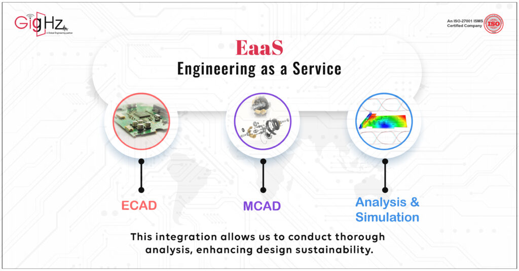
As the demand for advanced and integrated engineering solutions continues to rise, our Engineering as a Service (EaaS) is truly leading the way.
By harnessing the power of ECAD, MCAD, and Analysis & Simulation, we’ve positioned ourselves at the forefront of the industry.
What’s really exciting is that we offer a complete, end-to-end engineering solution, covering every step of the process.
This holistic approach isn’t just meeting today’s needs—it’s shaping the future of engineering.
And honestly, it’s an exciting time to be part of it all!
Why we do?
We challenge our Engineering capabilities with emerging technologies to keep your time and cost in control, thereby transforming product design with human touch quality.
Conclusion
It is clear that designing a Printed Circuit Board (PCB) in today’s technological world comes with numerous challenges and the need to utilize all of the resources available. Exploring PDN essentials for PCB designers is an essential part of managing such complex designs and avoiding costly errors.
With the ever-shifting landscape of technology, it is important to ensure you are taking advantage of the latest PDN approaches and maintain an eye on trending components.
There are plenty of resources out there for those looking to excel in PCB design, but landing on the right advanced PDN sets can make a huge difference in design time, cost, and overall product efficiency.
Now get here and explore the new domains of design possibilities.info@gighz.net