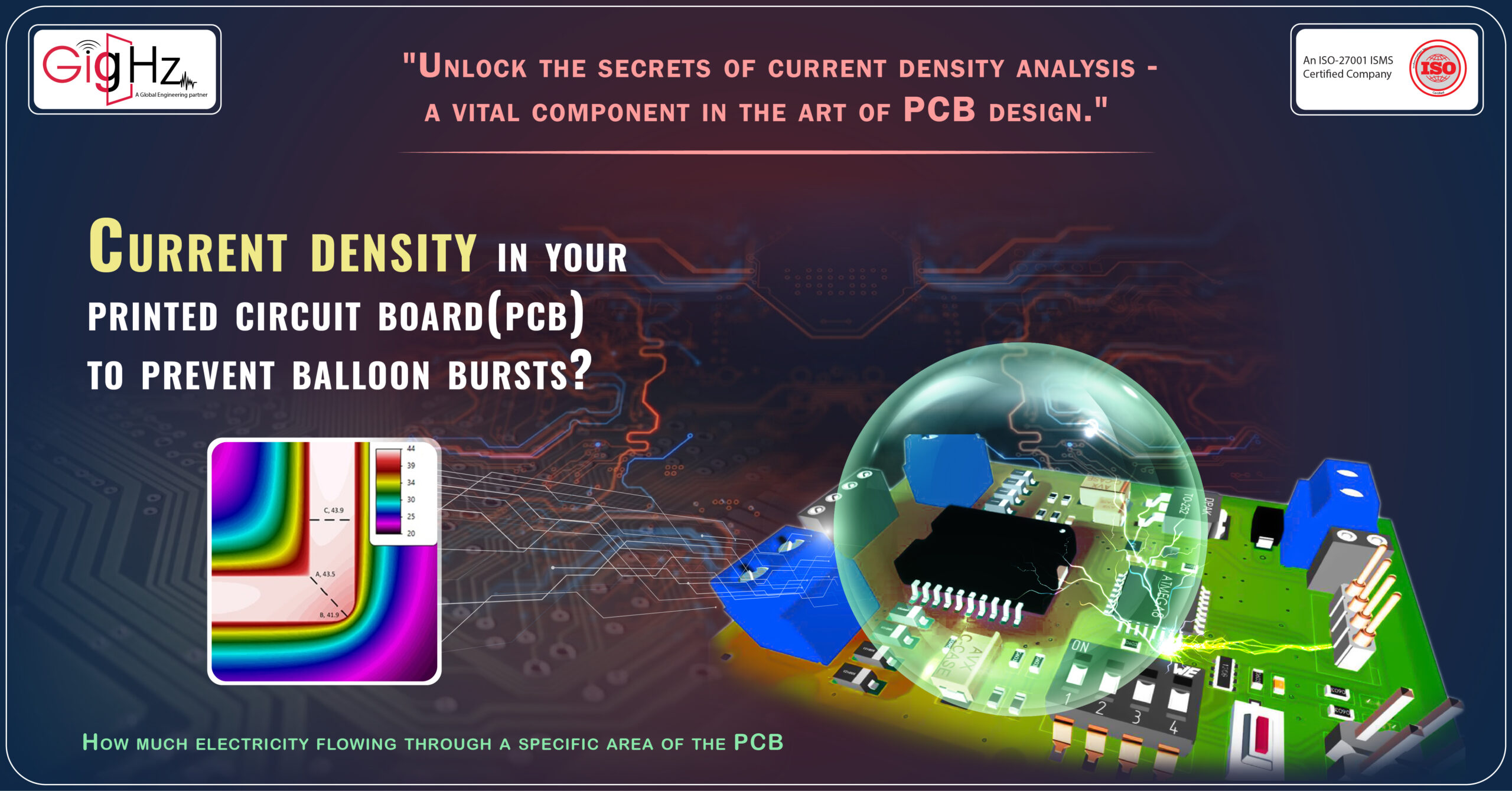
Considering these 5 needs of current density in your printed circuit board(pcb) to prevent balloon bursts?
Hello, dear seekers of inspiration!
As the sun gently painted the sky with hues of gold and pink in one of the most recent mornings, I found myself captivated by the enchanting dance of light and the promise of a brand-new day.
It’s moments like these that remind us of the boundless beauty that surrounds us, sparking a sense of wonder and curiosity within our hearts.
Category :
Published Date :
March 12, 2024
Category :
Published Date :
March 12, 2024
Category :
Published Date :
March 12, 2024
So, as we bask in the glow of the Smileful sunrise,
let’s embark on a collective journey of discovery and joy, right here.
In the world of electronic design, understanding how electricity moves through printed circuit board (PCB traces are super important.
One key thing we focus on is the “current density,” which tells us how much electricity is flowing through a specific area of the PCB,
The concept of current density in a PCB trace can be likened to the pressure within a balloon.
Just as you aim to maximize the air inside the balloon, exceeding the limit leads to a burst!
We dive into this technical stuff to make sure our PCB designs are strong and to prevent issues like the balloon bursts.
So, first of all, what exactly does the term ‘PCB trace’ refer to?”
PCB traces are like the intricate pathways on a printed circuit board (PCB) that carry electrical signals and power between electronic components.
Think of them as the “wires” of the PCB, but instead of being actual physical wires, they’re typically made of copper and are etched or printed onto the surface of the board.
These traces form a crucial part of the PCB’s functionality, enabling the flow of electricity between different components such as resistors, capacitors, integrated circuits, and so on.
By carefully routing and designing these traces, engineers and designers create the electrical connections necessary for the circuit to operate as intended.
The width, thickness, and layout of these traces play a vital role in ensuring that the PCB operates reliably and efficiently.
Factors such as current carrying capacity, signal integrity, and electromagnetic interference can all be influenced by the design of these traces.
We delve into the intricacies of current density to safeguard our PCB designs and avert potential issues that could impact the functionality of electronic devices.
By leveraging advanced tools and techniques, we meticulously analyze and optimize current density to strike the right balance between efficient current flow and thermal constraints.
Additionally, by exploring the relationship between current density and trace width, we ensure that our PCB traces can carry the required current without exceeding safe limits.
This meticulous approach not only prevents trace damage but also safeguards the overall integrity of circuit board components.
“Let’s get immersed in this!”
What's the deal with Current Density in PCB Traces?
So, when you’re diving into designing printed circuit board (PCB) traces, current density is a big deal.
It’s all about the amount of current flowing through a specific area of a trace.
J = I / A
Where,
J denotes the current density in amperes/meters squared (A/m2)
I is the current in amperes (A)
A is the cross-sectional area (m2)
Why does this matter so much?
Well, because it has a direct impact on how reliable and functional that trace is going to be.
Here’s the kicker:
If the current flowing through a trace is too high, things can start heating up in a not-so-good way.
We’re talking about increased resistance, voltage drops, and even the risk of the copper trace delaminating.
But hold on,
if the current density is too low, you might end up with thicker traces that eat up ` on the PCB, bumping up those manufacturing costs and putting a dent in your design flexibility.
So, to nail the design of PCB traces with just the right current density,
you’ve got to take into account things like the trace width, thickness, and the amount of current it’s going to handle.
You’ll also want to think about the ambient temperature and how well your PCB can dissipate heat.
By crunching the numbers for trace width and thickness based on the expected current, you can set yourself up for a PCB that operates reliably and efficiently.
Maintaining an appropriate current density in PCB traces is essential for avoiding thermal issues and optimizing the performance and reliability of electronic circuits.
It requires careful consideration of various factors to ensure that the traces can carry the desired current without causing overheating or other detrimental effects.
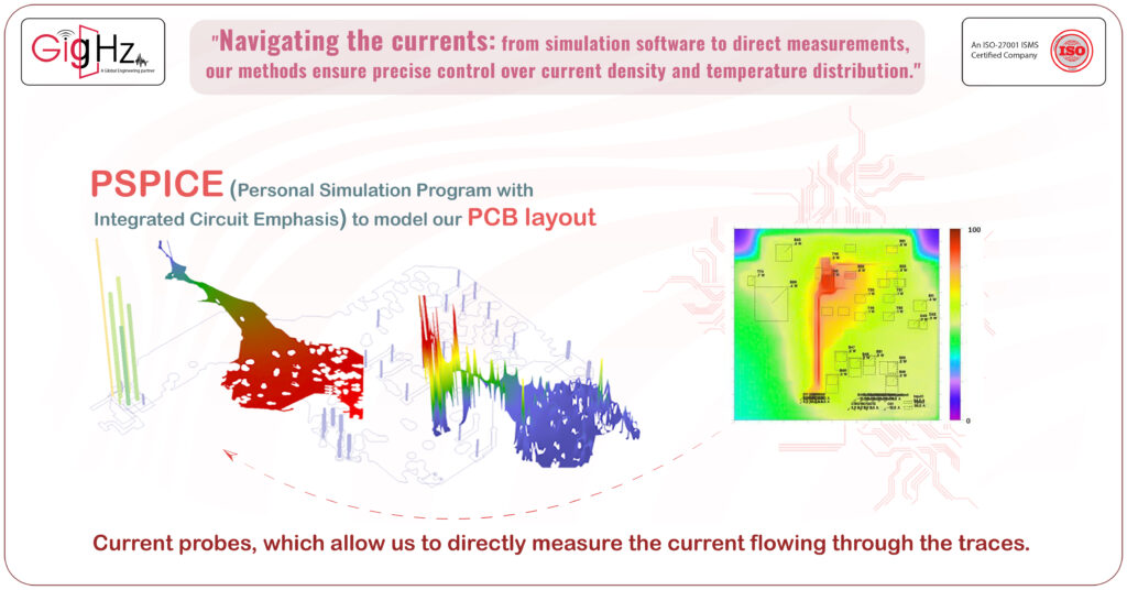
How We Analyze the Current Density in Our PCB Traces?
One notable issue was the presence of numerous undercuts in the design, which made traditional manufacturing methods costly and inefficient.
To overcome this, we explored alternative manufacturing techniques, such as 3D printing.
By utilizing 3D printing machines, we were able to eliminate the need for costly tooling and reduce production costs significantly.
The use of 3D printing allowed for greater design flexibility and eliminated the limitations imposed by traditional manufacturing methods.
Additionally, 3D printing enabled us to achieve a higher level of accuracy, with tolerances as low as 0.4mm.
This ensured that the medical device enclosures met the necessary requirements for functionality and quality.
Through value engineering, we were able to optimize and required to make the design of the medical device enclosure, reducing production costs from $385 per unit to $250 per unit.
This cost reduction not only improved the financial viability of the product but also made it more accessible to healthcare providers and patients.
By leveraging innovative manufacturing techniques and challenging the status quo, we were able to enhance efficiency and cost-effectiveness in the production of medical device enclosures.
This demonstrates the power of value engineering in driving innovation and improving the overall success of medical device manufacturing.
"Considering these 5 needs of current density in your printed circuit board(pcb) to prevent balloon bursts"

To prevent balloon bursts in your printed circuit board (PCB), it’s crucial to address the following 5 needs of current density:
Proper Trace Width Sizing: Adequate trace width is essential to ensure that the current density within the traces remains within safe limits.
Calculating the required trace width based on the maximum current flow prevents excessive current density, minimizing the risk caused by overheating.
Effective Thermal Management:
Efficient heat dissipation mechanisms, such as thermal vias and copper pours, are vital for managing current density-induced heat buildup.
By optimizing the thermal conductivity of the PCB and effectively dissipating heat, the risk of balloon bursts due to localized hotspots can be mitigated.
Material Selection and Dielectric Properties: Choosing materials with suitable dielectric properties and a high glass transition temperature (Tg) helps maintain the structural integrity of the PCB under high current density conditions.
This prevents by ensuring the PCB to withstand the thermal and mechanical stresses associated with elevated current densities.
Consideration of Current Carrying Capacity:
Understanding and adhering to the current carrying capacity of the PCB traces and conductive elements is critical.
By ensuring that the PCB’s conductive paths are designed to handle the expected current levels, the risk of current density-related failures, is minimized.
Thorough Electrical Design Verification:
Rigorous electrical design verification, including simulation and analysis of current flow and density, aids in identifying potential areas of concern related to current density.
This proactive approach allows for preemptive adjustments to the PCB layout or design before they occur.
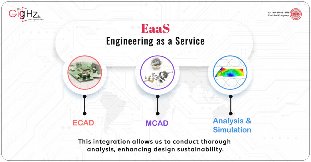
Our Significant Evolution: Engineering as a Service (EaaS)
Absolutely!
With the increasing prevalence of intricate engineering challenges, our Engineering as a Service (EaaS) offering is undeniably enhancing its impact.
We are harnessing the collective capabilities of ECAD, MCAD, and Analysis & Simulation, positioning us as frontrunners in the industry.
What’s especially thrilling, is our provision of an all-encompassing solution that spans the entirety of the engineering workflow.
It’s genuinely exhilarating!
Why we Do?

We challenge our ECAD capabilites with emerging technologies to keep your time and cost in control, thereby transforming product design with human touch quality by,
- Preventing Overheating: By monitoring and managing current density, we prevent localized heating which can lead to material degradation and ultimately bubble bursts.
- Ensuring Signal Integrity: Proper current density management is crucial for maintaining signal integrity, as excessive current density can introduce unwanted electromagnetic interference (EMI) and compromise the functionality of the PCB.
- Extending Lifespan: Managing current density effectively contributes to extending the lifespan of the PCB by minimizing the risk of premature failures caused by excessive current flow.
- Enhancing Reliability: Optimal current density distribution enhances the overall reliability of the PCB, reducing the likelihood of unexpected failures during operation.
- Compliance with Standards: Adhering to recommended current density guidelines ensures that our PCB designs meet industry standards for reliability and performance.
Conclusion
In the world of PCB design, it’s absolutely crucial to pay close attention to the essentials of managing current density.
We’re talking about things like getting the right trace width and spacing, using effective heat dissipation methods, selecting materials that can handle the heat, making sure our components can handle the current, and thoroughly testing everything to ensure it can stand up to the demands.
By taking these measures, we’re not just optimizing the current density in our PCB traces, we’re also reducing the risk of power failures and ensuring that our PCB design is not just safe, but also fully functional. It’s all about keeping things running smoothly and reliably, and these steps are key to achieving that goal.
Find Your Perfect Solution. Peruse Our Services Now! https://gighz.net/services/
As we navigate through these complex matters, it’s essential to seek comprehensive perspectives and reliable sources to comprehend the multifaceted implications.
Start Your Success Journey – Book a Call! https://calendly.com/gighz/30min