Why PCB footprints are crucial for successful electronic design?
- Posted On:
- August 13, 2024
- Category:
- Ecad

PCB Footprints
Just like how a footprint on the ground shows where a person or animal has stepped, a PCB footprint shows where each electronic component will be placed on the board.
Each component type has a unique shape and size for its connections (pads or pins) on the PCB.
These shapes are akin to footprints because they leave a distinct mark on the board.
PCB footprints are like templates or outlines on a printed circuit board (PCB) that show where and how each electronic component will be placed and soldered onto the board.
Imagine them as the designated spaces and shapes where components like resistors, capacitors, and microchips will sit.
Each electronic part has specific shapes and sizes for its metal connections (pins or leads).
The footprint ensures these parts fit perfectly onto the board, aligning their connections with solder pads.
The pads on the footprint connect the electronic parts to the copper tracks that carry electrical signals across the PCB.
These connections must be just right to ensure good electrical performance.
By following these footprints, manufacturers can place components accurately using machines.
This precision is crucial for making sure the board works correctly once it’s assembled.
Knowing the exact size and shape of each part’s connections (pins or pads) so they fit snugly.
Determining how far apart each part and its connections should be from others to avoid electrical interference.
Choosing materials that can handle the heat and electrical currents flowing through them without breaking down.
Consider designing the PCB Footprint for the
Designing them well is crucial for creating electronics that perform as expected and last a long time.
Ready, set go! for more details!
Things to know about PCB footprints
Have Your Datasheets at the Ready
In a detailed datasheet, you’ll see a drawing of the component showing its size, where to place it on the circuit board, and other important details needed for creating the footprint on the board.
Some components, especially power MOSFETs, might have a built-in heat sink or special attachment that should be included in the footprint design.
This is crucial for designs involving high voltage or high speed as these features are considered in thermal and electrical tests.
Which Data Is Integrated into PCB Footprints?
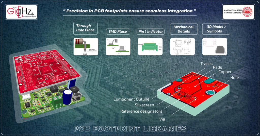
Pad or Hole Placement: This detail signifies the location of SMD component pads or through-hole component holes crucial for soldering, necessitating accurate definition.
Component Outline: This is described as a safeguarding area or perimeter within the PCB footprint, preventing component overlap and dictating the component’s shape.
Reference Designator: An alphanumeric identifier distinguishing the component in schematics and PCB layout, exemplified by markers like R75 for resistors and LD3 for LEDs.
Pin 1 Indicator: This is essential for components with numerous pins, like ICs, to avoid assembly confusion. It is particularly vital for QFP or DIP package components, often represented by a circle in diagrams.
Mechanical Details: Some components feature mechanical elements or extensions that could lead to clashes or overlaps with adjacent components, notably seen with heat sinks.
3D Model and Symbols: Each PCB footprint is linked to schematic symbols and frequently includes a 3D model, facilitating the creation of a comprehensive board model for confirming component positioning and spatial relationships.
PCB footprint libraries

A PCB footprint library is like a collection of templates for electronic components, ensuring that every piece fits perfectly onto the circuit board. This consistency makes designs more reliable and easier to assemble.
Instead of designing each component’s layout from scratch every time, you can pick from the library, saving you time and allowing you to focus on making sure your circuit works well.
Each footprint in the library is tested and verified to ensure that components solder onto the board correctly, guaranteeing proper connections and expected circuit functionality.
Libraries also aid in manufacturing by including details on how to solder components correctly, reducing mistakes and making mass production smoother.
The library follows industry rules and standards, ensuring your designs comply with safety and quality guidelines. In essence, a PCB footprint library is your toolbox for building electronic circuits—it makes designing easier, faster, and more reliable.
Whether you’re designing gadgets, cars, or anything with electronics, having a good library ensures your creations are solid and function as intended.
Why PCB footprints are crucial for successful electronic design?

1. Detailed Component Placement and Alignment
PCB footprints are meticulously designed to ensure precise placement and alignment of components. This involves:
Pad Geometry: Determining the size, shape, and spacing of pads for each component’s leads or terminals. This is crucial for achieving proper soldering connections during assembly.
Courtyard Definition: Specifying the minimum clearance area around each component to prevent solder bridges or interference with neighboring components.
Orientation and Rotation: Defining the correct orientation and rotation angle of components ensures they align with the PCB’s signal flow and mechanical constraints.
2. Electrical Performance Optimization
The dimensions and layout of PCB footprints significantly impact electrical performance:
Signal Integrity: Trace widths and pad sizes affect impedance matching, signal attenuation, and electromagnetic compatibility (EMC). Maintaining controlled impedance paths is critical for high-speed digital signals and RF applications.
Thermal Management: Thermal vias, pads, and heat sinks integrated into footprints help dissipate heat from power components, enhancing reliability and preventing thermal runaway.
3. Manufacturing Considerations
Efficient PCB manufacturing relies on well-designed footprints:
Design for Assembly (DFA): Footprints optimized for Surface Mount Technology (SMT) include appropriate pad sizes and solder mask clearances to facilitate automated pick-and-place assembly and solder paste application.
Design for Test (DFT): Including test points within footprints simplifies PCB testing and debugging processes, ensuring functional and electrical testing can be performed efficiently.
4. Compliance with Standards and Specifications
Adhering to industry standards ensures consistency and compatibility across designs:
IPC Standards: IPC-7351 provides guidelines for standardizing PCB footprints based on component type and package dimensions. These standards optimize pad geometries and ensure compatibility with assembly equipment and manufacturing processes.
Component Library Management: Maintaining a comprehensive library of standardized footprints allows designers to quickly select and integrate components into new designs, reducing errors and design iterations.
5. Design Flexibility and Scalability
Well-designed footprints support design flexibility and future scalability:
Modularity: Modular footprints enable designers to reuse common components across different PCB designs, promoting design consistency and reducing development time.
Footprint Generators: Automated tools and scripts can generate footprints based on component specifications, ensuring accuracy and consistency while adapting to evolving design requirements and component updates.
Final Thoughts
When it comes to creating a new PCB, having the correct footprints and 3D models for components is crucial.
By using a PCB design software like Altium, you can access libraries, which offers the largest PCB CAD library with footprints and models for millions of components.
With tools like Library Loader, you can easily install these libraries and get the PCB footprints and schematic symbols you need to create a new component.
If you’re looking to create a custom footprint or need to simulate your design, these resources make it easy to do so efficiently and accurately.
When working on your next PCB project, make sure you have access to the right tools and resources to ensure your design is successful.
By utilizing the correct PCB footprints and 3D models, you can save time and avoid errors in your component creation.
Whether you’re a seasoned engineer or new to the field, having access to these resources in the right file format is essential for creating a functional and accurate PCB.
Stay updated on our services—connect with our founder on LinkedIn: https://www.linkedin.com/in/chandra-thimma/recent-activity/all/
Table of Contents
Latest Post
Get Customized Engineering CAD Design Service

Lorem ipsum dolor sit amet, consectetur adipiscing elit. Ut elit tellus, luctus nec ullamcorper mattis, pulvinar dapibus leo.
Book a Free Consultation Call
Partner with Gighz and bring your most innovative design concepts to life. Our engineering cad services accelerate development so you can focus on your big vision.