Power Integrity Analysis in PCB Design: A 3-Step Roadmap
- Posted On:
- July 2, 2024
- Category:
- Analysis & Simulation
Power Integrity Analysis(PI)
While you are traveling on the road in your car, did you notice that?
You can look at the mirror and find something that looks kind of like a lense.
You could have blind spot detection, which is usually found on your side mirrors with the sensor built-in to the mirror.
That will be the sensor for that sides blind spot.
The notification for it is usually on the mirror itself and you can see when it works when you have someone next to you yet behind in another lane next to you.
Not only the blind spot detection, but also the other advanced features in ADAS,
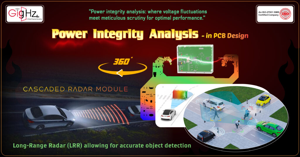
Well, let me introduce you to the unsung hero behind the scenes: the cascaded radar module.
This tech gem is like the silent protector in the world of Advanced Driver Assistance Systems (ADAS), ensuring everything runs smoothly to keep us safe on the road.
Imagine a world where sensors and processors work round the clock to safeguard drivers.
The cascaded radar module plays a key role here, teaming up with cameras, lidar, and other sensors to give your car a 360-degree view of its surroundings.
It’s all about precision, especially with long-range radar (LRR) beam-forming, allowing for accurate object detection even in challenging driving conditions.
These radar systems are no ordinary tech—they’re smart and versatile.
By using multi-mode cascaded radar data processing, they can detect and track objects effectively.
Plus, with cutting-edge tech like MIMO, which creates numerous virtual channels, these radar systems excel at recognizing obstacles and keeping us safe on the road.
When it comes to safety features like autonomous emergency braking or blind-spot monitoring, radar transceivers and SoCs step in to save the day.
These components are the powerhouses behind functions that help prevent accidents and make our driving experience smoother and stress-free.
“How the cascaded radar sensor module operates effectively is through the accurate flow of power integrity within the module.”
“We have analyzed the power integrity of the cascaded radar sensor module.
Based on our experience, let us share a 3-step roadmap for power integrity analysis.“
What Power Integrity Analysis Problems Can Occur in a PCB?
Power integrity analysis in PCB design involves a deep understanding of various aspects such as power delivery, impedance, voltage levels, and signal integrity.
One of the major complexities is ensuring a stable power rail and power distribution network to meet the power requirements of the circuit.
With the increasing complexity of power supplies and power distribution in modern circuit boards, the pcb designer must carefully consider the power planes and signal return paths to avoid power integrity problems.
Another challenge is performing accurate power integrity analysis through simulation and pcb layout using specialized design software like HyperLynx.
The pdn design and optimization of ac power integrity plays a crucial role in ensuring good power integrity and a good signal integrity throughout the PCB editor.
This involves considering multiple power sources, dc power supply requirements, and the overall power distribution network in the design process.
Power Integrity Challenges we faced
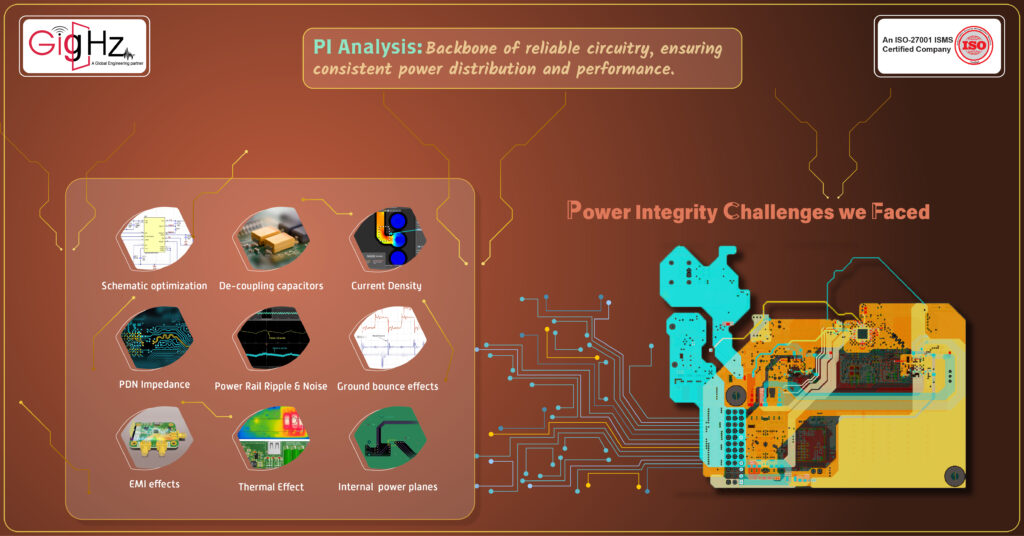
Following are the list of challenges involved in the Power Integrity Analysis that we faced,
- Schematic optimization: Ensuring the layout aligns with optimal electrical schematics for performance.
- Placement of De-coupling capacitors: Strategically positioning capacitors to manage noise and voltage fluctuations.
- Voltage Drop, Current Density & Via Current: Addressing issues related to voltage drop, current distribution, and via currents within the layout.
- PDN Impedance: Managing Power Delivery Network impedance for efficient power distribution.
- Power Rail Ripple & Noise: Mitigating fluctuations in power supply lines for stable operation.
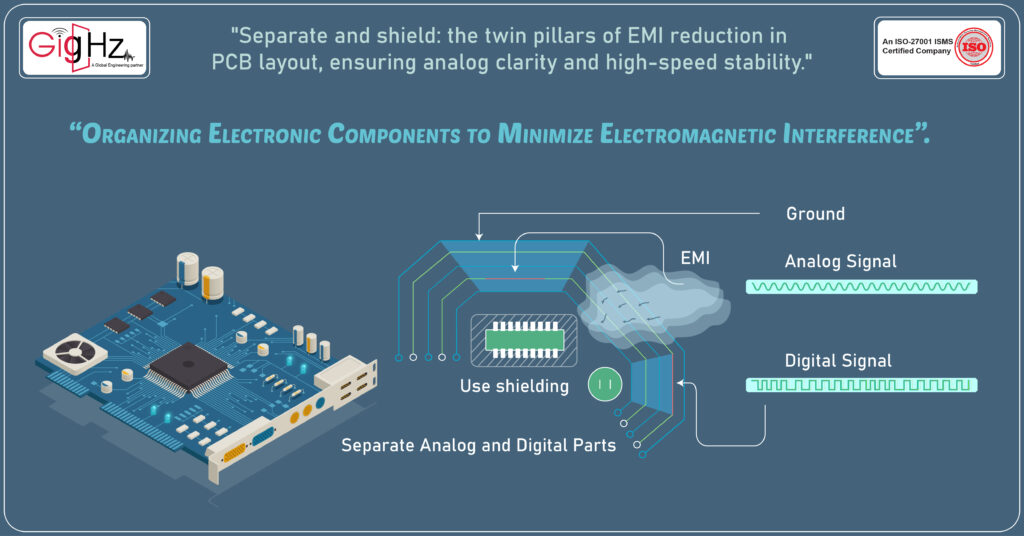
- Ground bounce effects: Minimizing ground signal disturbances for signal integrity.
- EMI effects: Controlling electromagnetic interference to prevent signal degradation.
- Thermal Effect: Addressing heat dissipation challenges for component longevity.
- Internal Resistance of power planes: Managing resistance in power planes for efficient power delivery.
- Frequencies Outages: Handling frequency disruptions to maintain operational stability.
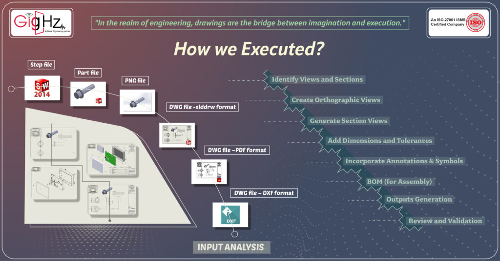
"Power Integrity Analysis in PCB Design: A 3-Step Roadmap"
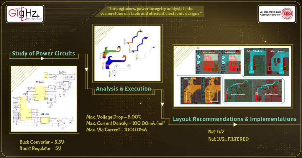
Study of Power Circuits:
In our project, we meticulously studied the power circuits to evaluate the performance of the power delivery network. The power circuits analyzed included:
- Buck Converter – 3.3V
- Boost Regulator – 5V
- 1V8
- 1V2
- 1V0_A
- 1V0_B
Analysis & Execution:
Utilizing the HyperLynx tool, we conducted a detailed analysis to assess the power integrity performance of the layout.
Problems within the power delivery network were identified from both DC (IR Drop) and AC (Frequency) perspectives. Key quantities calculated included:
- Current Density: XX mA/mil²
- Voltage Drop: XX V
- Via Current: XX mA
Analysis – Plots and Results:
For various nets such as +1V2, +1V2_FILTERED, FE1_VRF1_FILTERED, and FE2_VRF2_FILTERED, we analyzed parameters including voltage, current, and requirements such as maximum voltage drop, current density, and via current.
Layout Recommendations & Implementations
Layout Recommendations:
To enhance PCB performance, we recommended and implemented tailored solutions. For example, for Net 1V2, recommendations included:
- Increase Cu pour width to XX mm
- Add vias at specific locations
- Adjust trace width on different layers
Layout Implementations:
These recommendations were incorporated into the PCB layout to improve performance. Implementations included increasing Cu pour widths, adding necessary vias, and adjusting trace widths on different layers as follows:
Net: 1V2
- Cu pour width increased to XX mm
- Vias added at specific locations
- Trace width adjusted on different layers
Net: 1V2_FILTERED
- Cu pour width increased to XX mm
- Trace width adjusted to XX mm on Layer X under component Y
Similar optimizations were applied to other nets to ensure optimal power delivery and circuit efficiency.
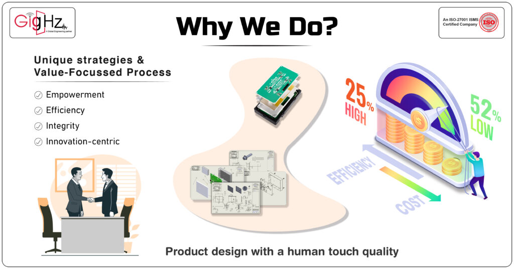
Why we Do?

Our commitment to this detailed Power Integrity Analysis stems from the critical role it plays in ensuring the robustness and efficiency of the power delivery network within radar sensor modules.
By addressing challenges such as layout optimizations, signal interference mitigation, and performance enhancements through strategic recommendations, we strive to guarantee the seamless operation of safety and driver-assistance systems in the automotive domain.
Our meticulous approach not only meets client demands but also aligns with industry standards for power integrity, enhancing the overall reliability and performance of radar sensor applications.
We challenge our Power Integrity Analysis capabilities in Automotive Industry to keep your time and cost in control with human touch quality.
Our Engineering as a Service (EaaS)
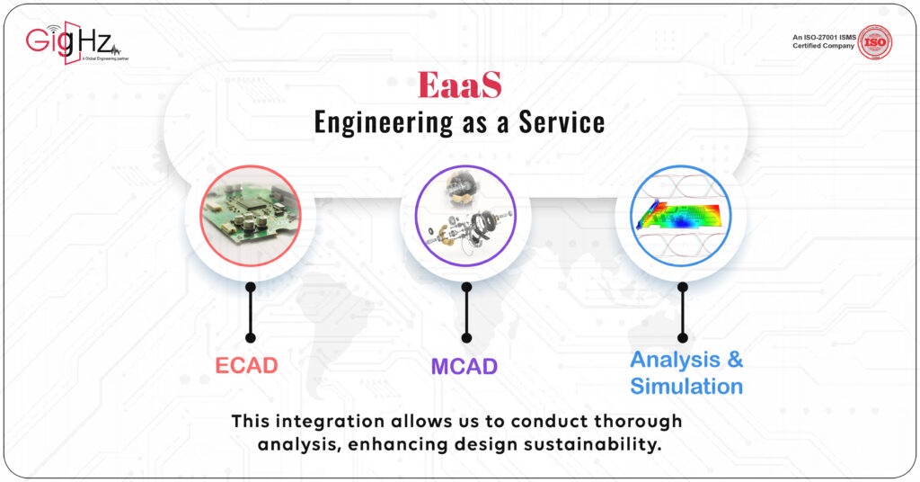
Absolutely! As the demand for advanced engineering solutions keeps growing, our Engineering as a Service (EaaS) is really stepping up its game.
We’re tapping into the power of ECAD, MCAD, and Analysis & Simulation, which positions us as frontrunners in the industry.
The fact that we offer a full package, covering every single step of the engineering process, is what makes our approach so exciting.
It’s this kind of forward-thinking approach that’s going to shape the future of our engineering,
It’s truly thrilling!
Conclusion
As we conclude our discussion on PCB power integrity, is effective for understanding the basics of power integrity and how to effectively perform power integrity analysis in your board design.
Addressing power and ground planes is crucial in ensuring stable power delivery and avoiding signal integrity problems.
By leveraging design tools and simulations, you can identify and resolve power integrity issues early in the system design phase, providing a solid foundation for the next PCB design.
Utilizing techniques, we analyze power and ground pins, power rail probes, and PDN in a PCB is essential to ensure power integrity throughout the power system.
Discover our Specialities. Visit our Services Page. https://gighz.net/services/
Power Integrity Analysis in PCB Design: A 3-Step Roadmap
Our Notable Upgrade: Engineering as a Service(EaaS)
Book a Free Consultation Call
Partner with Gighz and bring your most innovative design concepts to life. Our engineering cad services accelerate development so you can focus on your big vision.
Related Blogs


