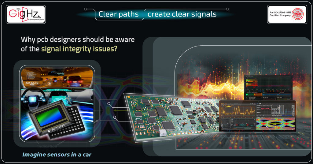
Why pcb designers should be aware of the signal integrity issues?
- Posted On:
- August 22, 2024
- Category:
- Analysis & Simulation
Signal Integrity Issues
In the world of printed circuit boards (PCBs), think of digital bits as tiny messengers carrying important messages from one place to another, like a well-coordinated team.
Signal integrity acts like a reliable guide, making sure these messengers reach their destination smoothly without getting lost or mixed up.
Now, let’s relate this idea to something we all know: cars.
Imagine sensors in a car sending critical information to the control units, similar to how messages move through a PCB.
Just as a car needs all its parts working in sync for a smooth ride, signal integrity ensures that data travels accurately between components in the vehicle, ensuring everything runs efficiently and safely.
In printed circuit boards, signal integrity is all about making sure digital signals move smoothly through the board without getting distorted.
Designers focus on matching signal paths with components, keeping things organized, reducing noise, and checking designs to guarantee signals work well in electronic devices.
This ensures that the signals stay strong and accurate as they travel around the board, ultimately making the electronics function properly.
SI is about digitally transmitting a signal, and then faithfully reproducing its copy at the receiving end by controlling the physical phenomena known to affect its quality.
Some of the phenomena that are so prevalent in any electronic design are related to the signal itself – its reflections, resonance, and the resulting Cross Talk.
Let’s dig in!
If the signal integrity is missing in the printed circuit board

Data Corruption: Imagine sending critical information from one component to another on a PCB, but due to poor signal integrity, some bits get flipped along the way. This can be likened to receiving a jumbled message where important details are distorted, leading to misinterpretation and errors in communication.
Signal Distortion: Picture a signal traveling through a PCB trace like a smoothly flowing river. However, with signal integrity problems, it’s as if rocks suddenly disrupt the flow, causing ripples and changes in the signal’s path. This disruption can result in signals arriving at their destination in a garbled or delayed manner.
Noise and Interference: Think of signal integrity as ensuring a clear phone call – but without it, imagine static interference distorting the conversation. Similarly, on a PCB, electromagnetic interference can introduce unwanted noise into the signal path, hindering the clarity and reliability of data transmission.
Timing Issues: Consider trying to synchronize dancers in a performance without proper timing cues. In a PCB system without adequate signal integrity, different components may struggle to coordinate their actions, leading to a disorganized and chaotic performance akin to missed data packets or communication failures.
Power Consumption: Visualize a car using more fuel than necessary to compensate for a faulty engine. Similarly, a PCB with signal integrity issues might require excess power to overcome signal distortions, leading to inefficiency, higher energy consumption, and potential strain on the system.
Compliance Challenges: Think of signal integrity compliance like following traffic rules – without adhering to them, chaos can ensue. Failing to meet signal integrity standards can result in electronic devices not meeting regulatory requirements, jeopardizing their safety, reliability, and market acceptance.
System Reliability: Envision a chain reaction where one weak link causes a series of failures in a machine. Similarly, compromised signal integrity in a PCB can lead to frequent malfunctions, unreliable performance, and premature component wear, ultimately impacting the overall quality and dependability of the electronic system.
To overcome these signal integrity issues, there is a need to understand the importance of signal integrity.
Understanding signal integrity in a PCB
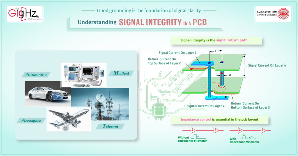
In PCB design, various industries like automotive, aerospace, medical, telecom, and others require specific considerations and tailored approaches to meet their unique requirements.
Signal integrity is crucial in a PCB design to ensure the reliability and performance of electronic systems.
High-speed designs are particularly susceptible to signal integrity issues such as signal loss, crosstalk, impedance mismatches, and ground bounce.
Impedance control is essential in the pcb layout to minimize signal reflections and maintain good signal integrity. Differential signaling and proper termination techniques can help mitigate signal distortion, signal degradation. Controlled impedance trace and power and ground plane structures are key elements in pcb design guidelines for high-speed design.
Signal integrity analysis and electromagnetic interference studies are often conducted to identify the root cause of signal integrity problems.
Another factor affecting signal integrity is the signal return path, which must be carefully designed to prevent signal reflections.
The electrical signal propagation along high-speed transmission lines is influenced by impedance, inductance, and ground plane design.
Power supply noise and power integrity problems can also lead to poor signal integrity and should be addressed in the circuit design.
Vias and flex pcb construction can introduce additional complexities in pcb fabrication that may impact signal integrity.
Why pcb designers should be aware of the signal integrity issues?
Challenges Faced by Designers:
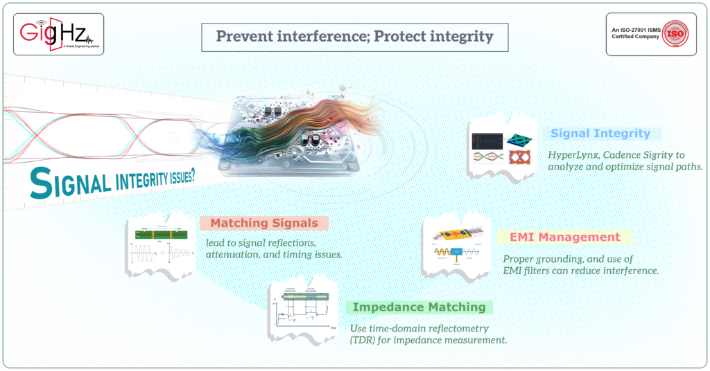
Matching Signals:
- Description: Ensuring proper impedance matching is critical to prevent signal reflections, which can cause signal degradation and loss of data integrity.
- Challenges: Improper matching can lead to signal reflections, attenuation, and timing issues that degrade system performance.
Signal Interference:
- Description: Crosstalk and electromagnetic interference (EMI) can arise when signals interact with each other or with external sources.
- Challenges: This interference can distort signals, leading to errors, reduced reliability, and compromised efficiency.
Layout Issues:
- Description: Poor PCB (Printed Circuit Board) layout and routing can cause a range of signal integrity problems.
- Challenges: Inadequate planning can result in increased parasitic capacitance and inductance, leading to signal delays and potential failure.
Best Ways to Manage Signal Quality:
Smart Wiring:
- Technique: Maintain organized and optimized routing of signal paths using appropriate trace widths and spacing.
- Benefits: Minimizes cross-talk and maintains signal strength and integrity.
Grounding Help:
- Technique: Implement solid and continuous grounding planes, and ensure proper grounding of components.
- Benefits: Reduces electrical noise and ensures a stable reference voltage, which helps maintain signal clarity.
Testing Tools:
- Technique: Use simulation and modeling tools (e.g., SPICE, electromagnetic field solvers) to predict signal behavior.
- Benefits: Early detection and resolution of potential signal integrity issues enhance overall system performance and reliability.
Deep Insights
Impedance Matching:
- Explanation: Impedance matching involves designing the signal path impedance to match the source and load impedances, reducing signal reflections.
- Tools and Methods: Use time-domain reflectometry (TDR) for impedance measurement and simulation software for design verification.
Crosstalk Mitigation:
- Explanation: Crosstalk occurs when signal paths are too close, allowing signals to couple with adjacent traces.
- Solutions: Increase spacing between traces, use differential pairs, and incorporate guard traces to mitigate crosstalk.
EMI Management:
- Explanation: Electromagnetic interference can be internal (from other components) or external (from environmental sources).
- Solutions: Shielding sensitive components, proper grounding, and use of EMI filters can reduce interference.
Thermal Management:
- Explanation: High-speed circuits can generate significant heat, affecting signal integrity.
- Solutions: Implement proper thermal management techniques like heat sinks, thermal vias, and adequate airflow design.
Parasitic Elements:
- Explanation: Unintended inductance and capacitance (parasitic) can affect signal integrity.
- Solutions: Minimize parasitic effects through careful PCB layout and by using low-parasitic components.
Signal Integrity Analysis:
- Explanation: Comprehensive signal integrity analysis includes simulation of signal paths to identify potential issues.
- Tools: Use SI simulation tools like HyperLynx, ADS (Advanced Design System), or Cadence Sigrity to analyze and optimize signal paths.
By addressing these challenges and employing these management strategies, designers can enhance signal integrity and ensure robust and reliable system performance.
Final Thoughts
In conclusion, maintaining signal integrity is crucial in high-speed digital design. Signal integrity requirements for HDI PCB design and circuit board construction must be carefully considered to increase signal integrity and prevent signal integrity issues.
The design process should include signal timing skew, signal traces, and system design in order to maintain signal integrity.
Signal integrity practices such as proper circuit simulator usage and following design rules can help mitigate many design issues that can be traced back to signal integrity problems.
Whether working with CMOS circuits, rigid-flex PCBs, or analog signals, understanding and implementing signal integrity design practices are essential for successful circuit board design.
To know more about our services, follow our founder through LinkedIn https://www.linkedin.com/in/chandra-thimma/recent-activity/all/
Table of Contents
Latest Post
Get Customized Engineering CAD Design Service

Book a Free Consultation Call
Partner with Gighz and bring your most innovative design concepts to life. Our engineering cad services accelerate development so you can focus on your big vision.