“VIP” Defined: A Closer Look at Printed Circuit Board(pcb) Design
- Posted On:
- July 2, 2024
- Category:
- Ecad
Via in Pad-PCB Design
As the sun sets and the sky turns a soft orange, imagine sitting down with a warm cup of coffee.
You can feel a light drizzle cooling the air around you.
The day is winding down, and you’re enjoying this peaceful moment of calm and quiet, surrounded by nature’s beauty.
“Peace” matters here, right!
“Just as we seek calmness in quiet times, finding peace is essential when designing PCBs.”
“Today, let’s take a closer look at Printed Circuit Board Design of Automotive ECU, by defining the VIP what we have done”.
So, what exactly the VIP in PCB design means for?
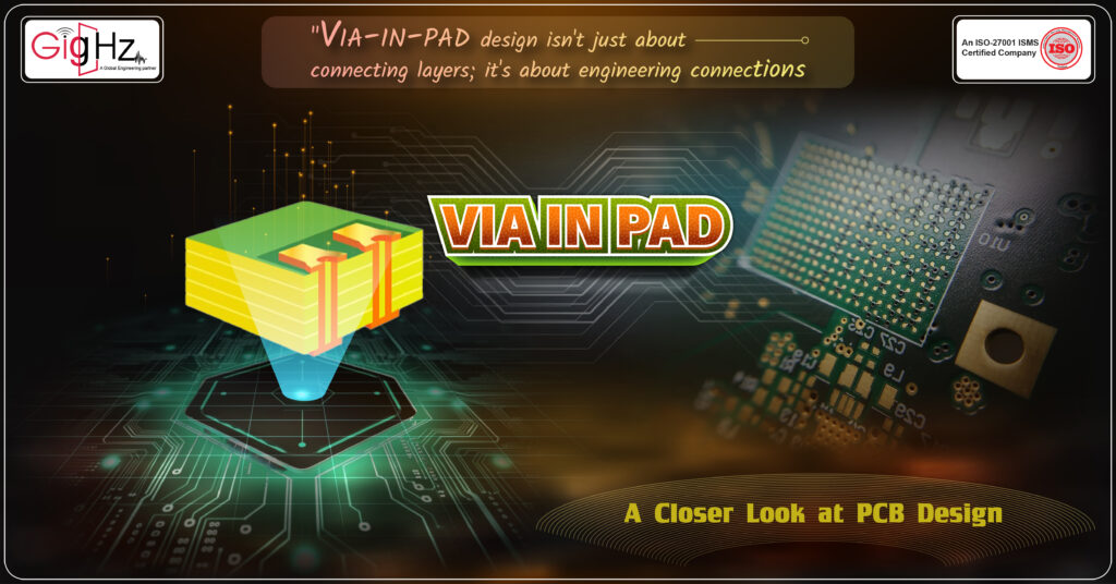
Its Via-In-Pad,
Consumers show a preference for compact electronic gadgets. Achieving smaller devices necessitates the use of diminutive electronic parts.
Given the tight spacing between component pads, conventional via routing may not always be feasible.
In such instances, designers turn to a technique called “via in pad” (VIP).
This approach involves positioning the via directly onto the copper pad of a surface-mounted component (SMD).
Via of the PCB Design
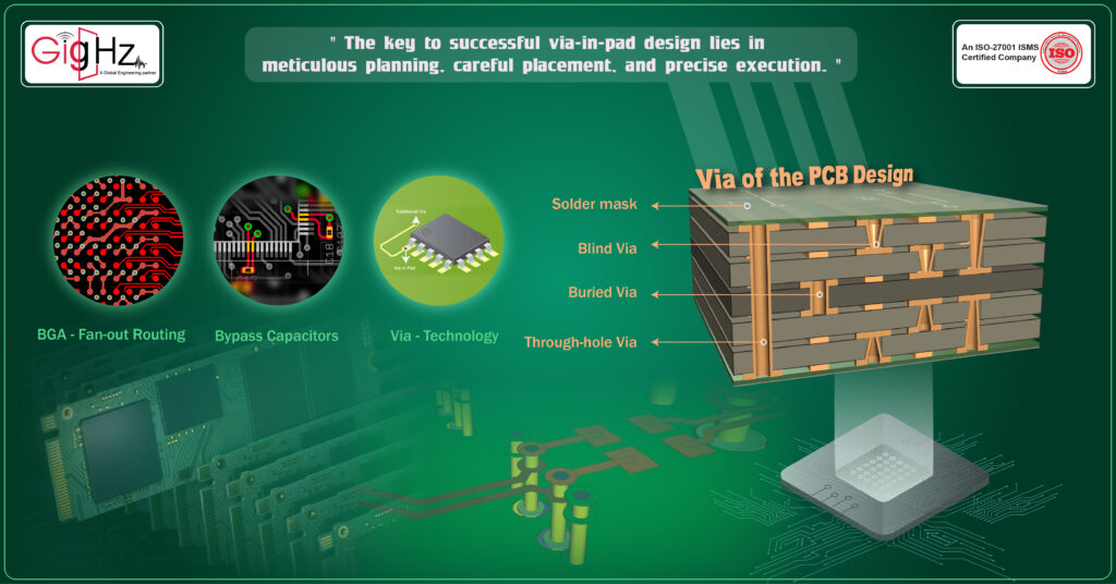
A via is like a tiny tunnel in a PCB that links the different layers together. It’s coated with a metal like copper to let electricity flow through and connect the layers. Vias are super important in PCBs with many layers because they help join the layers for both electricity and heat.
Vias can go through the whole board to link all layers or just pathway to connect only some layers.
Their size and shape depend on what the PCB needs. Vias can be round or not, and their width can vary a lot.
Where you put vias in a PCB is really crucial. It’s best to place them where there aren’t important parts or wires because they might mess up signals or cause electrical issues.
Also, where vias are placed can affect how well the board deals with heat, so it’s smart to think about heat needs when deciding where to put vias.
Via-in-Pad of the PCB Layout Design
Via-in-pad refers to drilling vias directly on pads. These pads are typically Surface Mount Device (SMD) pads sized 0603 or larger, or Ball Grid Array (BGA) pads. They are commonly referred to as VIP (via in pad). Vias on through-hole component pads do not fall under via-in-pad because those vias are necessary for inserting and soldering the component leads.
As electronic products trend towards being lighter, thinner, and smaller, PCBs are also progressing towards higher density and complexity.
Consequently, electronic components are shrinking in size too. For example, BGA components now come in smaller packages with reduced pin pitch.
The available space between BGA pins for routing can be extremely limited, necessitating vias for transitioning between layers in routing.
In cases where the BGA pin pitch is too small for fan-out routing, drilling vias in pads becomes the sole viable option. Another scenario arises when bypass capacitors are positioned behind a BGA component with densely packed pins, making it impossible to route vias without intersecting any pads.
This situation mandates drilling vias in capacitor pads. Hence, there are two categories of via-in-pad: on BGA pads and on SMD pads.
It is advisable to steer clear of via-in-pad designs whenever possible in routing layouts. Boards with via-in-pad configurations generally incur high manufacturing costs and longer cycle times.
"VIP" Defined: A Closer Look at Printed Circuit Board(pcb) Design for Automotive ECU
Design Guidelines we follow
Via-In-Pad Necessary
When considering via-in-pad necessity, it is crucial to check the via hole size before embarking on BGA fan-out. Failure to assess the proper via size can lead to fan-out issues or produce inaccurate results.
Design via-in-pad configurations when the BGA pin pitch is too small for standard fan-out practices. In such cases, route BGA pins through alternative layers or from the component side.
Do not require Via-In-Pad
Routing for fan-out should precede layer routing in the design process. When dealing with BGA fan-out layouts, especially in scenarios where the pin count is high and routing space is limited, ensure that vias are centrally positioned between BGA pads.
Typical parameters for BGA fan-out include a via diameter of 0.15-0.2mm, trace width of 3-4mil, and an annular ring of 0.3-0.4mm. This results in a minimum BGA pin pitch for effective fan-out routing of 0.35mm.
Design Considerations while we Designing the Layout Process
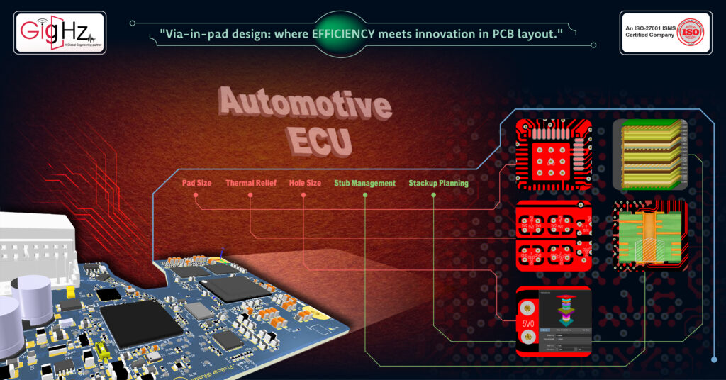
When creating via-in-pad PCB designs for Automotive ECU pcb, we encounter various benefits and constraints that shape the layout process:
- Pad Size: Introducing a via hole to a pad in Automotive ECU pcb designs necessitates increased pad size, potentially leading to spacing challenges or pad overlap.
- Capture Pad: It may require a capture pad on inner layers to protect the via barrel, utilizing additional board space.
- Thermal Relief: Implementing a thermal relief cutout around the via in Automotive ECUs is crucial for managing heat dissipation, thereby expanding the pad area.
- Plating Reliability: Ensuring robust plating of the via-pad connection in Automotive ECUs is vital to reduce reliability risks, sometimes requiring adjustments in design and processes.
- Hole Size: The via diameter in Automotive ECU pcb should be smaller than what the component permits but large enough to accommodate plating thickness.
- Alignment: Precise layer-to-layer alignment in Automotive ECU pcb needs to correspond with pad size and tolerance requirements specified by the via location.
- Stackup Planning: Aligning the layer transition facilitated by the via with routing needs in Automotive ECUs significantly influences stackup design.
- Stub Management: Effective coordination of via length with the layer transition point is essential in minimizing via stubs in Automotive ECU pcb designs.
- Manufacturing Process: The assembly and board fabrication processes for Automotive ECU pcb must effectively support design intricacies like hole size, plating, and accuracy.
It is advisable to steer clear of via-in-pad designs whenever possible in routing layouts. Boards with via-in-pad configurations generally incur high manufacturing costs and longer cycle times.
Key info about Via In Pad in Printed Circuit Board Design
Via In Pad is a crucial aspect of printed circuit board (pcb) design that involves placing a via directly on a pad to optimize space utilization and increase routing options.
When it comes to pcb manufacturing, this design process requires careful consideration of design rules, circuit design, and component placement to ensure a successful outcome. Pcb designers must utilize design software with design rule checks to accurately implement pcb design guidelines and design for manufacturability within the layout process.
Integrated circuits play a significant role in determining the number of layers needed for a pcb, as well as the board size and the side of the pcb that will be utilized. Whether it’s a rigid pcb or a multilayer board, considerations for pcb component placement and manufacturing and assembly are vital throughout the pcb design steps
Designing a new pcb requires a comprehensive understanding of electronics industry standards, pcb design concepts, and design tools Altium Designer on Altium 365.
By following a meticulous design and layout approach, pcb designers can create a high-quality bare board that meets the requirements of the pcb industry.
For those new to pcb design, an introduction to pcb provides a comprehensive guide to pcb design, covering everything from schematic creation to manufacturing files, ensuring a seamless transition from concept to printed circuit board assembly.
Our Memorable Achievement: Engineering as a Service (EaaS)

Definitely!
As complex engineering challenges become more prevalent, our Engineering as a Service (EaaS) offering is truly elevating its presence.
We are leveraging the combined strengths of ECAD, MCAD, and Analysis & Simulation, which establishes us as leaders in the field.
What’s particularly exciting is that we provide a comprehensive solution, encompassing the entire engineering workflow.
It’s genuinely exhilarating!
Conclusion
From a design perspective, incorporating vias in pads is akin to traditional vias with a slight variation. The key distinction lies in the necessity of an additional manufacturing file that specifically includes the vias within component pads requiring filling and capping. At times, simply informing the PCB manufacturer about the desired vias to be implemented as via in pad suffices.
It is crucial to consider the pad diameter as a significant factor. The chosen via size must adhere to the minimum annular ring specifications outlined by IPC Class 2 or Class 3. Additionally, the pad size of the via should be sufficiently large to accommodate manufacturing tolerances.
Discover our Specialties. Visit our Services Page https://gighz.net/services/
“VIP” Defined: A Closer Look at Printed Circuit Board(pcb) Design


Our Notable Upgrade: Engineering as a Service(EaaS)
Book a Free Consultation Call
Partner with Gighz and bring your most innovative design concepts to life. Our engineering cad services accelerate development so you can focus on your big vision.
Related Blogs