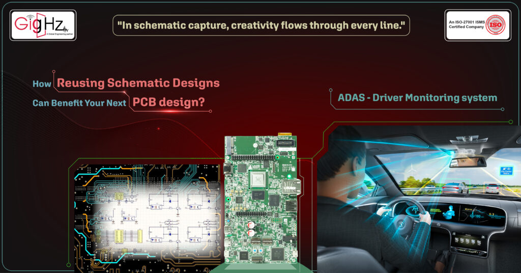
How Reusing Schematic Designs Can Benefit Your Next PCB design?
- Posted On:
- July 9, 2024
- Category:
- Ecad
Printed Circuit Board (PCB) Design Schematic Capture
The word “reuse” in daily life has a positive impact and is associated with sustainability, efficiency, and resourcefulness.
In our day-to-day tasks, it can have a significant impact on us,
don’t you think?
Reusing existing work is a key factor in reducing the amount of time and effort required for any project, right.
As we venture into PCB Design Layout, the importance of PCB Schematic Capture becomes apparent.
How does schematic capture impact the PCB design layout,
The importance of schematic capture in PCB design layout cannot be overstated.
It serves as the blueprint for the entire design process, guiding engineers from concept to reality while ensuring accuracy, efficiency, and successful project outcomes.
Now, a question arises: how can we repurpose an existing schematic design?”
By understanding the way that design reuse works, you enable a greater ability to creatively smarter, more effective uses of your time.
Lets share how we done these work,
We designed the schematic capture by reusing for the pcb layout of the Driver Monitoring system used in an ADAS application.
So sit back, relax and be prepared to be amazed—it’s show time!
Lets dig in!
Front-End Electronic Design and Schematic Capture
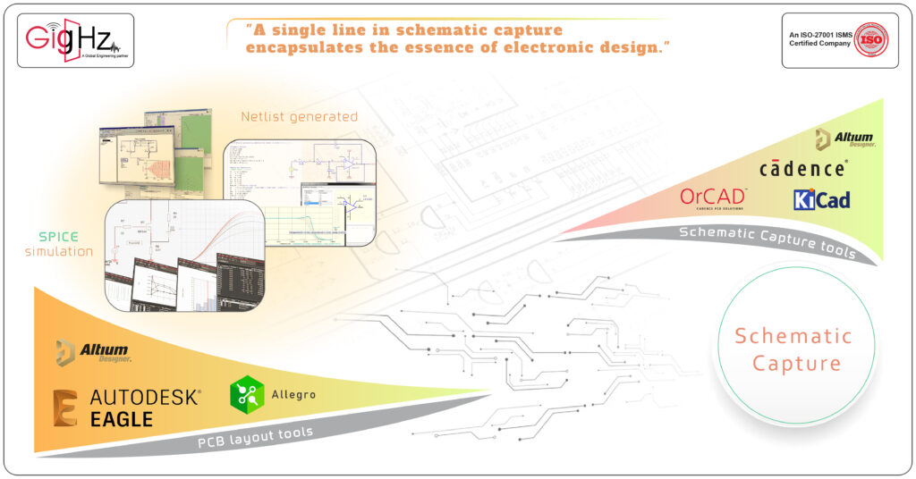
Front-end electronic design and schematic capture involve the creation of electronic circuits and schematics using specialized software tools.
This process starts with our engineer’s design intent and involves utilizing Schematic Capture tools such as Cadence, Altium, KiCad, or Orcad to create a visual representation of the circuit.
In this stage, the schematic editor is used to place schematic symbols and connect them together to define the functionality of the circuit.
Once the schematic is complete, it can be used for simulation using tools like SPICE to verify the design before moving on to the pcb layout stage.
The netlist generated from the schematic capture process is then imported into the pcb design software to start the pcb layout. This involves placing components on the board and routing the traces to create the printed circuit board (PCB).
During the pcb layout stage, design constraints, mechanical requirements, and integration with other systems need to be taken into account.
PCB layout tools like Altium, Allegro, Eagle, or Autodesk are commonly used for this purpose.
Once the pcb layout is complete, the final design can be exported for manufacturing and prototyping.
Schematic Design Reuse with Hierarchical Schematics for PCB Layout
When it comes to schematic capture and pcb layout, utilizing hierarchical schematics can greatly improve productivity and reduce errors in our board design.
By reusing schematic sheets in a library and connecting them through nets, the designer can quickly create complex circuits.
With spice simulation and circuit simulation, we can simulate the circuit design before moving on to pcb layout. This can help identify potential issues early on and ensure a smoother pcb editor process.
A hierarchical schematic is where different areas of functionality are represented on the top sheet of the design project by block symbols.
Each block symbol is linked to a separate design that is incorporated into the master design. By selecting and opening a block symbol, you will open up its linked design.
The schematic tool will manage these different designs, including their nets and reference designators, so that there aren’t any data conflicts. The end result is that all of the linked designs are merged into the master design.
This functionality lends itself to design block reuse very well.
Take, for instance, a power supply that was created as a hierarchical schematic for an existing design.
When a new design requires that same power supply, it can simply be added as a referenced schematic. In the new design a block symbol is created that links to the existing power supply schematic.
Once the block symbol is placed, the new design will pull in an instance of the power supply schematic and synchronize the nets and references designators.
All that’s left is to connect the desired nets to the power supply block symbol ports.
How Reusing Schematic Designs Can Benefit Your Next PCB design?
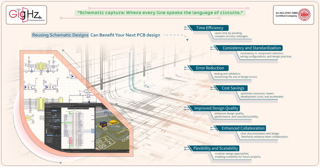
- Time Efficiency: Reusing schematic designs saves time by eliminating the need to recreate complex circuitry. This time-saving benefit allows designers to focus on critical design aspects like layout optimization and signal integrity analysis.
- Consistency and Standardization: Reusing proven schematic designs ensures consistency in component selection, wiring configurations, and design Standardization across projects simplifies maintenance, reduces errors, and enhances overall design coherence.
- Error Reduction: Reused schematics have undergone rigorous testing and validation, minimizing the risk of design errors. This leads to a more reliable PCB design with fewer bugs and issues, improving overall product quality and reliability.
- Cost Savings: Schematic reuse reduces design iteration cycles and minimizes redundant work. This cost-effective approach optimizes resources, lowers development costs, and accelerates time-to-market for new products.
- Improved Design Quality: Leveraging successful schematic designs enables the incorporation of best practices, optimizations, and lessons learned from previous projects. This iterative improvement process enhances design quality, performance, and manufacturability.
- Enhanced Collaboration: Reused schematics provide a common platform for collaboration among team members. Clear documentation and familiarity with existing designs facilitate communication, knowledge sharing, and collaborative problem-solving within design teams.
- Flexibility and Scalability: Reusing schematics allows for modular design approaches, enabling scalability for future projects. Modular design blocks can be easily integrated, modified, and expanded upon, providing flexibility to adapt to evolving project requirements.
By technically leveraging schematic reuse, engineers can streamline the design process, reduce design risks, optimize resources, and drive innovation through cumulative design knowledge and experience.
Our Schematic Capture Design Services
As a vital step in the hardware design process, schematic capture becomes an interaction between designers and specialized tools.
Aligned with your specifications, our team leverages dedicated schematic creation and refinement tools.
We generate compatible netlists for various simulation and PCB layout packages, amplifying design adaptability.
Additionally, errors in the schematic can be rectified through the integration of component datasheets.
We also specialize in:
- Manual Schematic Capture
- PCB design services
- Multi-Tier Hierarchical Design
- Schematic Optimization
- Schematic and Layout Integration
- Electrical Rule Checking
- Error-Free Schematics
- Schematic Reuse
- Cable Harness Schematics
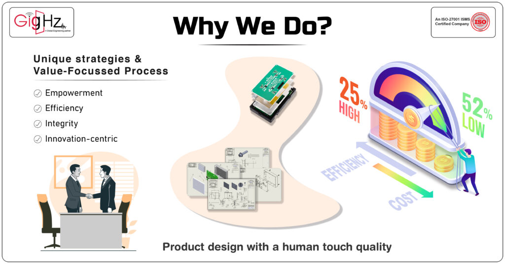
Why we do? GigHz DNA
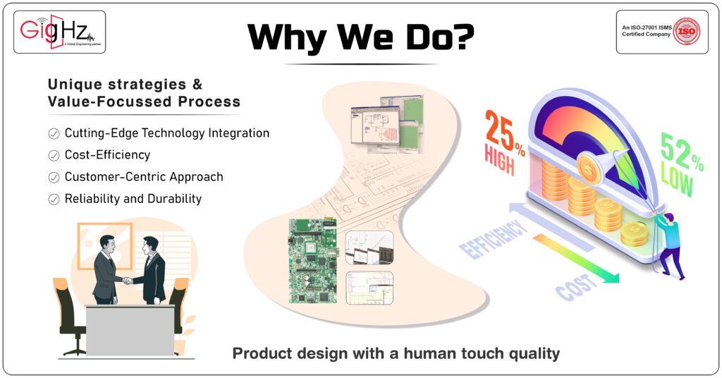
We challenge our Engineering ECAD capabilities with emerging Automotive technologies to keep your time and cost in control, thereby transforming product design with human touch quality.
Despite the challenges in technology, we stand out from the competition due to our innovative methods and value-driven process.
This approach enables us to achieve a significant cost reduction of 52% while simultaneously increasing operational efficiency by 25%.
Conclusion
In essence, using Altium Designer is a great choice for designing your PCBs due to its open-source nature and the numerous features available.
With its built-in Spice simulator, 3D viewer, and connectivity features, offers a comprehensive solution for ECAD design.
Although it may take some time to learn, the open-source community and resources available can help speed up the learning process.
It also allows users to collaborate easily, customize design rules, and manage their supply chain through the BOM and connector features.
Overall, these reuse ideas form a powerful CAD system that meets the needs of designers and provides an efficiency for PCB design.
Discover our Specialities. Visit our Services Page. https://gighz.net/ecad-services/
How Reusing Schematic Designs Can Benefit Your Next PCB design?
Our Notable Upgrade: Engineering as a Service(EaaS)
Book a Free Consultation Call
Partner with Gighz and bring your most innovative design concepts to life. Our engineering cad services accelerate development so you can focus on your big vision.
As we conclude our discussion on PCB power integrity, is effective for understanding the basics of power integrity and how to effectively perform power integrity analysis in your board design.
Addressing power and ground planes is crucial in ensuring stable power delivery and avoiding signal integrity problems.
By leveraging design tools and simulations, you can identify and resolve power integrity issues early in the system design phase, providing a solid foundation for the next PCB design.
Utilizing techniques, we analyze power and ground pins, power rail probes, and PDN in a PCB is essential to ensure power integrity throughout the power system.
Discover our Specialities. Visit our Services Page. https://gighz.net/services/
Related Blogs