The 10 Most Common Causes of PCB Failure – And How to Avoid Them
- Posted On:
- May 15, 2025
- Category:
- Ecad

You spent months creating your flawless PCB but testing revealed its failure because traces melted down, components heated up, and signals became chaotic. Frustrating, right?
You’re not alone. Even experienced engineers and hobbyists can experience PCB failures which affect designers, who take great care with their designs.
What’s the truth?
Small oversight mistakes lead to most failures which evolve into major system breakdowns. Your traces did not have enough thickness to handle the current passing through them. Thermal management appears to have been neglected in the final design specifications.
A wrongly positioned via allowed the solder to move away leading to an unstable connection.
The good news?
Using this knowledge you can build boards with durability and reliability at the beginning of your design process.
In this guide, we’ll uncover the 10 most common PCB killers—issues like poor trace width, thermal nightmares, and grounding disasters—that sabotage even well-planned projects. More importantly, we’ll give you practical, actionable fixes to dodge these traps. These insights will help you avoid both prototyping and production problems that save you time while reducing project costs.
The time has come to fortify your printed circuit board designs. Let’s dive in.
The 10 Most Common Causes of PCB Failure
1. Inadequate Trace Width
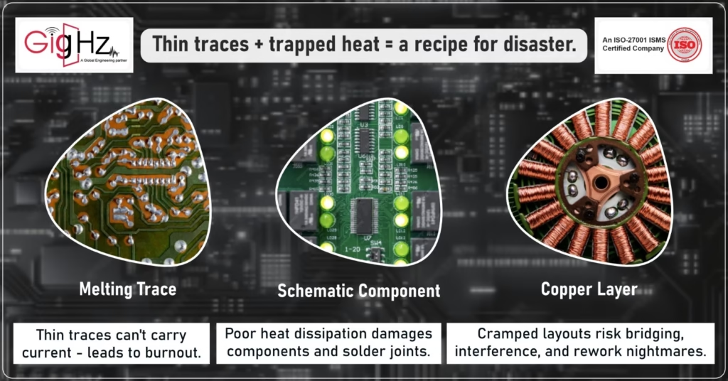
Small trace dimensions represent a common reason for PCB failure, since they cannot handle the current effectively. Trace under sizing leads to overheating that creates thermal stress, delamination, and may result in full trace destruction. The problem becomes most severe in power supplies and motor driver systems due to high current flow.
Following IPC-2152 standards enables users to determine the right traces width for their specified current needs. High-current paths require either wider traces or thicker copper layers (typically 2 oz versus 1 oz) or external busbars as an added heat dissipation method. Manufacturers can identify future thermal hotspots through simulation tests before they start production.
Poor Thermal Management
PCBs succumb to silent death when heat exposure causes component failures, solder joint debonding, or board distortion.
A lack of effective thermal management occurs when designers use insufficient copper heatsinks or fail to include thermal vias or do not provide sufficient airflow in sealed designs.
The implementation of thermal vias beneath power-intensive components including MOSFETs and voltage regulators helps minimize thermal problems.
The vias provide heat dissipation channels that direct heat to both internal and bottom layers. Thermal relief pads help solder joints by improving the soldering process without reducing heat dissipation effectiveness.
The solution for severe situations includes the implementation of metal-core PCBs or the addition of heat sinks to protect critical components.
3. Inadequate Component Spacing
Components which are positioned too near each other result in solder bridging and signal interference. It creates obstacles for assembly and rework. High-density design layouts face special difficulties because of their constrained dimensions.
The IPC-7351 guidelines offer specifications for component spacing that prevent problems from occurring.
Maintain proper distances between high-voltage traces to stop arcing from occurring. Designers who adopt 3D modeling before manufacturing can find and address mechanical system conflicts beforehand.
4. Incorrect Pad Sizes or Footprints
Inadequate pad dimensions and faulty footprint designs lead to solder joint weaknesses and both tombstoning and positioning errors among components. The use of generic CAD library footprints instead of manufacturer-recommended dimensions leads to this common design problem.
You should always check that pad dimensions match those provided in the component datasheet. The use of footprint libraries that conform to IPC standards guarantees precise results. Surface-mount components such as QFNs and BGAs need thermal pads using correct stencil designs to achieve reliable soldering results.
5. Under-pad placement of Vias
Solder wicking occurs when vias are positioned directly under component pads because molten solder flows into the vias instead of creating proper joints. The connection integrity suffers thus leading to component breakdowns particularly in BGA packages.
Tent the vias with solder mask to prevent solder wicking, when they need placement under pads. When soldering BGA packages use the via-in-pad technology to create flat surfaces via filled and capped vias. Any vias should be placed outside of high-stress areas which include connector pads.
6. Signal integrity problems due to inaccurate impedance control
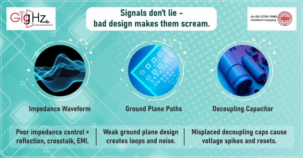
The precise control of impedance remains crucial for high-speed signals which exist in USB, HDMI, and DDR memory interfaces. When traces lack proper alignment the signals can produce reflections that generate crosstalk and EMI, thus causing unpredictable system behavior or full circuit malfunction.
You can find the right traces dimensions for your design using impedance calculators available through PCB Toolkit. Make sure your PCB manufacturer validates that dielectric materials together with stackup design will fulfill impedance requirements. Short high-speed signal paths should be placed at a distance from noisy electronic components.
- The improper design of grounding components and return paths
The quality of a ground system design affects noise generation, creates ground loops, and EMI that disrupts both analog and digital circuits. A common problem stems from grounds that split or insufficient return paths.
Using a strong ground plane structure will decrease impedance levels. When designing for mixed-signal systems implement star grounding techniques to isolate analog from digital ground domains. High-frequency signals need a low-impedance return path located directly below the trace to minimize both loop area and EMI issues.
- Improper Decoupling Capacitor Placement
Power supply voltages gain stability through decoupling capacitors that filter high-frequency noise. The improper placement or insufficient quantity of decoupling capacitors can cause voltage spikes that reset microcontrollers and produce unpredictable behavior.
IC power pins should be connected to decoupling capacitors located as near as feasible to their pins. Multiple capacitors should be used (0.1µF and 10µF) to filter high frequencies and bulk noise respectively. Maintaining short connections between capacitors and integrated circuits helps reduce inductance.
- Poorly layered stacked component
Unbalanced PCB stackups lead to assembly warping and impedance mismatches as well as increases EMI levels. Multilayer designs highly depend on correct layer arrangement because improper positioning affects signal integrity and thermal performance.
A symmetrical layer stackup arrangement should include Signal-GND-PWR-Signal layers in 4-layer boards to stop the board from warping. The placement of high-speed signals between ground planes within internal layers helps decrease EMI. Reach out to your PCB manufacturer for help in designing a stackup configuration suitable for your product needs.
10. Failure to perform proper Design Rule Checks (DRC)

Design Rule Checks (DRC) failures cause manufacturing issues which include unconnected nets, insufficient clearances and missing solder mask openings. Designed improperly these issues trigger both costly rework requirements and boards that do not function properly.
The design process requires an automated DRC check before reaching the final stage. The design tool allows users to create special rules for high-voltage traces and RF sections as well as high-current paths. Verify that both solder mask and silkscreen display accurate readable information.
Final Thoughts: Engineering best practices for designing reliable PCBs
- Design phase prevention of PCB failures becomes achievable through proactive methods.
- Run modeling simulations for crucial elements such as thermal performance and signal integrity and power delivery systems.
- Collaborate with your PCB manufacturer to verify both stackup design and materials selection.
- Complete testing along with visual inspections, flying probe evaluations, and functional testing activities.
Addressing these ten typical causes of PCB failures allows for higher reliability together with reduced rework costs and better performance outcomes for your boards.
CTA- Book a consultation call
For quality PCB manufacturing, resolving PCB defects and professional collaboration contact us.
For more updates on PCB and resolving manufacturing issues you can follow us at- https://www.linkedin.com/in/chandra-thimma/
Latest Post
Get Customized Engineering CAD Design Service

Book a Free Consultation Call
Partner with Gighz and bring your most innovative design concepts to life. Our engineering cad services accelerate development so you can focus on your big vision.