A functional PCB sits on your desk — but the original design files are missing.
There’s no schematic, no layout data, no Gerber files, and no clear documentation. Yet the product still needs to operate reliably, meet performance targets, and support future upgrades.
Do you redesign the board from scratch?
Or recover the intelligence already engineered into it?
This is where PCB reverse engineering becomes essential.
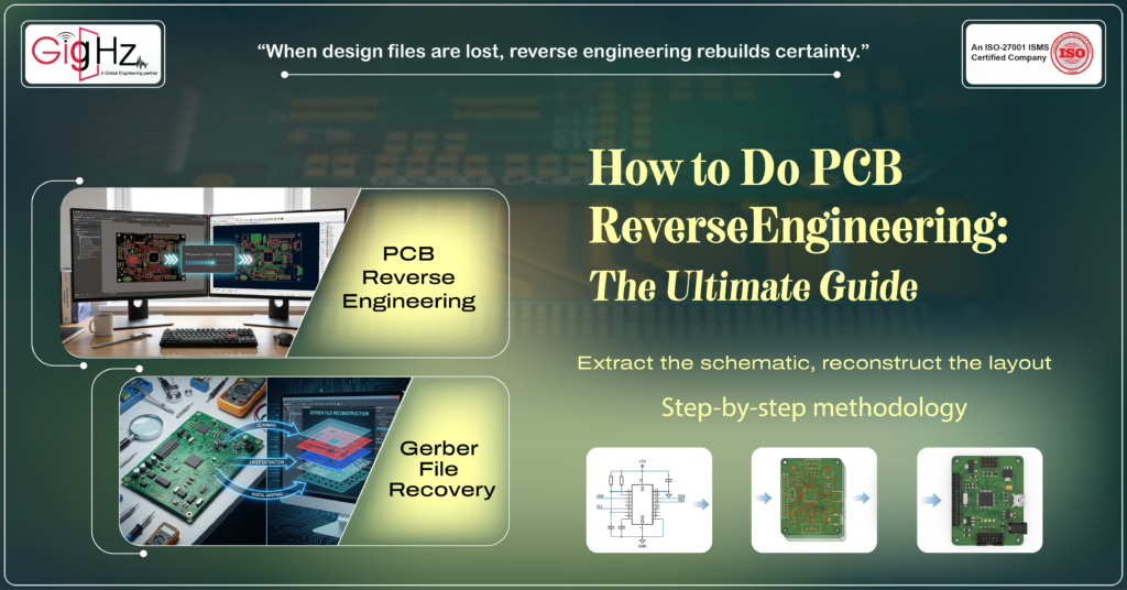
In many cases, the goal includes Gerber file recovery, allowing accurate manufacturing data to be recreated from the physical board. Engineers then extract the schematic, reconstruct the layout, and rebuild complete manufacturing documentation. When executed methodically, this process helps replace obsolete components, resolve performance limitations, restore lost documentation, and extend overall product lifecycle with reduced technical risk.
In this guide, you’ll learn the complete step-by-step methodology — clearly and practically so you can apply it confidently to real-world hardware challenges.
Understanding PCB Reverse Engineering
PCB reverse engineering is the structured process of analyzing an existing printed circuit board to recreate its schematic, layout, material stackup, and overall design intent.
You’re not just redrawing traces.
You’re rebuilding the logic behind the hardware.
Engineers typically use it when:
- Design files are missing
- Documentation is incomplete
- Components are obsolete
- Performance issues need investigation
- A PCB redesign is planned
- Compliance documentation must be recreated
Instead of starting from zero, you start from what already exists — and work backward intelligently.
When done correctly, the output includes:
- Complete schematic diagrams
- Reconstructed PCB layout files
- Updated Bill of Materials (BOM)
- Manufacturing-ready documentation
- Verified performance data
That’s far more valuable than just copying a board.
Core Principles Behind PCB Reverse Engineering

Step 1: Initial Inspection & Documentation
Before any electrical analysis begins, document the physical board.
You can:
- Draw it manually (for simple boards)
- Scan it
- Photograph both sides using a high-resolution camera
Best practices:
- Use a dark background to prevent light bleed through vias
- Ensure uniform lighting
- Capture both top and bottom layers clearly
- Maintain correct scale reference
For complex PCBs, image cleanup may require:
- Cropping
- Colour correction
- Contrast adjustment
- Background removal
- Layer isolation
Proper image preparation prevents errors during layout reconstruction.
Step 2: Prepare and Edit the Image
Once captured, upload the image into editing or vector conversion tools.
Typical editing steps include:
- Cleaning tracks for clarity
- Marking non-plated holes
- Enhancing solder pads
- Removing noise or background artifacts
- Converting bitmap images to vector format
For multilayer boards, each side must be processed separately.
The goal is to create a clean visual representation that accurately reflects copper traces and pad geometry before layout reconstruction begins.
Step 4: Bill of Materials Extraction
Now move into detailed documentation.
Record:
- Part number
- Manufacturer
- Package type
- Pin configuration
- Datasheet reference
- Functional purpose in the circuit
Understand each component’s role:
- Is this regulator part of a feedback loop?
- Is this capacitor for decoupling?
- Is this IC handling signal conversion?
Accurate component identification ensures reliable schematic reconstruction and supports obsolete component replacement decisions.
Step 5: Trace Connectivity and Extract the Netlist
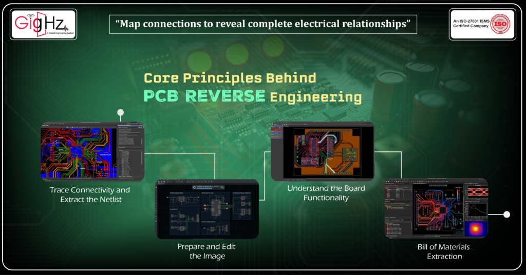
During this stage, engineers perform PCB netlist extraction to digitally verify connectivity and ensure that every traced signal matches the actual board.
Trace:
- Power nets
- Ground planes
- Signal paths
- Differential pairs
- High-current traces
- Clock lines
For multilayer PCBs, advanced techniques may include:
- Layer inspection
- PCB scanning
- X-ray imaging
- Controlled delayering
This transforms visual inspection into electrical analysis.
Step 6: Rebuild the Schematic
This stage is often referred to as PCB schematic reconstruction, where the board’s electrical intent is recreated digitally inside an EDA software.
Group by functional blocks:
- Power management
- Microcontroller
- Communication interfaces
- I/O circuits
- Protection circuits
Do not copy physical placement.
Rebuild electrical logic.
Validate:
- Signal direction
- Power distribution
- Ground strategy
- Control flow
- Pin-to-Pin Connections
Validation ensures there are no missing nets or incorrect assumptions.
Now the board’s logic becomes visible.
Step 7: Reconstruct the PCB Layout
The first step in layout reconstruction is preparing the design outline. The outline defines the board boundary, component zones, routing regions, and layer organization before detailed reconstruction begins.
This phase, often called PCB layout reconstruction, focuses on accurately rebuilding trace routing, via placement, and layer stack-up based on the original board geometry.
This includes:
- Route traces
•Component placement
• Via placement
• Copper pours
• Layer stack-up
• Plane structures
This helps reproduce the electrical and physical layout behavior of the original PCB.
Observe:
- Trace width for current capacity
- Length matching for high-speed signals
- EMI-sensitive region isolation
- Return path management
- Controlled impedance traces
- High-speed routing constraints
- Differential pair matching
Layout analysis reveals performance priorities embedded in the design.
Step 8: Validate Before Final Output
Before you modify anything, validate the reconstructed board carefully. This prevents copying hidden design flaws.
Run:
- Connectivity consistency check
- Electrical Rule Check (ERC)
- Design Rule Check (DRC)
- Signal integrity analysis
- Power integrity evaluation
- Thermal simulation
- Current density analysis
If flaws exist in the original design, this step exposes them — allowing improvement rather than duplication of errors.
Bottom Line
The reverse engineering process is not just a recovery technique.
It’s a disciplined engineering process that allows you to:
- Understand legacy designs
- Replace obsolete components
- Improve performance
- Rebuild missing documentation
- Transition safely into redesign
Instead of guessing, you analyze.
Instead of starting from scratch, you build from insight.
Instead of copying blindly, you engineer with intent.
When done methodically, PCB reverse engineering becomes one of the most valuable tools in product development and lifecycle extension.
Book a Call. Schedule a Free Consultation now. https://calendly.com/gighz/30min
Stuck in a loop of challenges? Always pick smart solution that works
Have you faced costly rework because 2D drawings skipped in MCAD workflows?
Effective way to prevent MCAD documentation errors recalls?
Please answer both poll questions before submitting.
Thank you for your response! 😊
Latest Post
Get Customized Engineering CAD Design Service

Book a Free Consultation Call
Partner with Gighz and bring your most innovative design concepts to life. Our engineering cad services accelerate development so you can focus on your big vision.