

PCB Analysis Before or After Layout: Which Matters More?
- Posted On:
- November 16, 2026
- Category:
- Ecad

The PCB layout is finished. Routing is complete. DRC is clean. The board looks ready for fabrication.
Then SI analysis finds a signal-integrity problem.
A power rail shows excessive impedance in PI analysis. A thermal simulation reveals a hotspot beneath a high-power component.
Now the engineering team has a difficult choice: change the layout and delay the release, or move forward and risk finding the problem during prototype testing.
This raises an important question:
Should PCB analysis happen before layout, after layout, or both?
The answer is both—but for different reasons.
Pre-layout analysis helps define what the PCB needs to achieve. Post-layout analysis verifies whether the actual layout achieves it.
That distinction can make the difference between designing around a requirement and redesigning around a problem.
How Does PCB Analysis Help Before Layout?
Before traces are routed, many electrical and thermal decisions are still flexible.
That makes early analysis valuable because it can influence the architecture rather than simply identify problems in an existing layout.
1. Stackup and impedance requirements
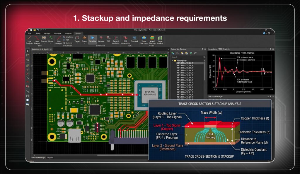
For high-speed interfaces, impedance is not something that should be checked only after routing.
The required impedance depends on factors such as:
- Trace width
- Copper thickness
- Dielectric thickness
- Distance to the reference plane
- Dielectric constant
- Routing layer
For example, if a high-speed interface requires controlled impedance, the stackup must provide a practical geometry for achieving that target.
If the stackup is finalized first and analyzed later, the required trace geometry may not fit the available routing space.
Pre-layout analysis therefore helps answer:
“Can this stackup support the electrical requirements before we start routing?”
That is much easier to solve than discovering the problem after thousands of traces have been placed.
2. Power Distribution Can Be Planned Early

The same principle applies to power integrity.
A PCB may contain multiple voltage domains, high-current devices, switching regulators, processors, memory, and sensitive analog circuitry.
Before layout, engineers can establish requirements for:
- Power and ground planes
- Decoupling strategy
- Current paths
- Via structures
- PDN targets
- Placement of high-current components
The goal isn’t to predict every detail of the finished board.
It is to prevent the layout from being built around an unsuitable power-distribution strategy.
3. Thermal Constraints Can Influence Placement

Thermal analysis also becomes more useful when it can influence component placement.
A high-power device placed in a congested area with limited copper and poor heat-spreading paths may create a thermal problem that becomes difficult to correct later.
Early thermal considerations can influence:
- Component placement
- Copper areas
- Thermal vias
- Heat-spreading paths
- Board-level airflow considerations
In other words, pre-layout analysis answers:
“What constraints should the layout team design around?”
What Changes After Layout?
Once routing is complete, the question changes.
You are no longer asking what the PCB should look like.
You are asking whether the PCB that was actually created will behave as expected.
This is where post-layout analysis becomes essential.
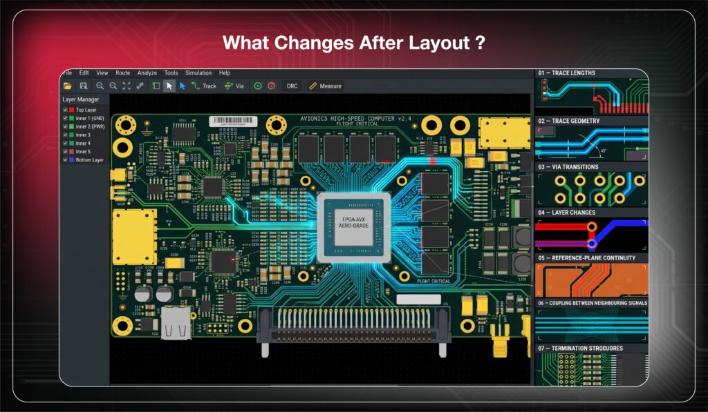
SI Analysis Validates the Actual Routing
Signal integrity depends heavily on physical implementation.
After layout, engineers can evaluate the actual:
- Trace lengths
- Trace geometry
- Via transitions
- Layer changes
- Reference-plane continuity
- Coupling between neighbouring signals
- Termination structures
A signal may meet schematic connectivity requirements and pass DRC while still producing excessive ringing, reflections, or crosstalk.
For high-speed interfaces, the physical routing is part of the electrical behavior.
That is why post-layout SI analysis cannot simply be replaced by early planning.
PI Analysis Checks the Real Power Network

The same applies to power integrity.
A PDN may look reasonable during planning but behave differently once the actual board structure is implemented.
Post-layout PI analysis can examine factors such as:
- PDN impedance
- Voltage distribution
- Current paths
- Plane structures
- Decoupling locations
- Resonant behavior
The location of a capacitor, the connection through vias, and the physical path between a device and its power source can all influence high-frequency performance.
The finished layout gives the analysis something concrete to evaluate.
Why Waiting Until the End Can Create Rework
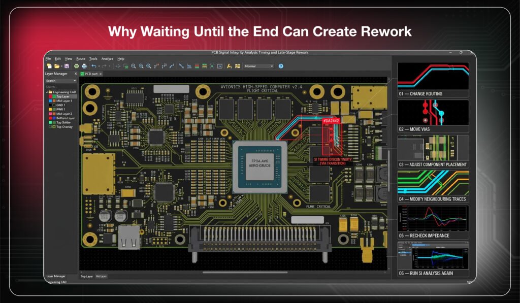
This is where the timing of analysis becomes important.
Imagine discovering after routing that a critical differential pair has an unacceptable discontinuity.
Fixing it might require:
- Changing the routing.
- Moving vias.
- Adjusting component placement.
- Modifying neighbouring traces.
- Rechecking impedance.
- Running SI analysis again.
One problem can therefore create a chain of changes.
The same thing can happen with power or thermal issues.
A hotspot discovered after placement may require component relocation. A PDN problem may require changes to capacitor locations or plane structures.
The later a fundamental problem is discovered, the more design decisions may depend on it.
So, Which Matters More?

Pre-layout analysis matters for prevention.
post-layout analysis matters for validation.
They are not competing approaches—they are two checkpoints in the same engineering process.
Pre-layout analysis defines constraints and design targets, while post-layout analysis verifies whether the implemented design meets them.
For example, pre-layout SI work helps establish stackup and impedance strategy, while post-layout SI analysis confirms whether the routed board actually meets electrical performance requirements.
The first guides the design. The second validates it.
Final Answer
So, before or after layout—which matters more?
Neither is sufficient by itself.
Running analysis only before layout can leave the actual implementation unverified.
Running it only after layout can turn preventable constraints into expensive rework.
The better approach is to use analysis according to the decision:
Before layout: What should we design for?
After layout: Did we achieve it?
That is the real value of PCB analysis—not simply finding problems, but finding them early enough to influence the design and late enough to validate the board.
Identify risks before fabrication.
Request a PCB analysis review.
Book a Call. Schedule a Free Consultation now. https://calendly.com/gighz/30min
Stuck in a loop of challenges? Always pick smart solution that works
Have you faced costly rework because 2D drawings skipped in MCAD workflows?
Effective way to prevent MCAD documentation errors recalls?
Please answer both poll questions before submitting.
Thank you for your response! 😊
Latest Post
Get Customized Engineering CAD Design Service

Book a Free Consultation Call
Partner with Gighz and bring your most innovative design concepts to life. Our engineering cad services accelerate development so you can focus on your big vision.
