


IPC’s electronics assembly quality benchmarks track rework and scrap as measurable costs of poor quality, alongside defect rates, yields, inspection methods, and customer returns. Its 2019 benchmark study covered 57 electronics manufacturers and OEMs worldwide.
Today, increasing design complexity and higher-speed electronics make preventing rework even more critical.
That matters because PCB rework is rarely just about fixing one trace.
When a problem appears after fabrication, engineers may need to debug the board, modify the layout, rebuild prototypes, repeat testing, and sometimes move to another board revision.
So what happens when a PCB passes design verification but still needs rework?
A high-speed interface may fail intermittently. A processor may reset under load. A power component may run hotter than expected.
The design passed the rules. The hardware still failed the test.
PCB Design Verification can confirm that a board meets defined design rules, but it does not guarantee performance under real operating conditions.
What Can Verification Still Miss?
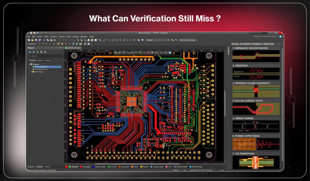
Consider a high-speed memory interface.
The schematic and layout are correctly connected. DRC passes. Trace widths and clearances meet the defined rules. The routing looks clean.
The board is fabricated.
During bring-up, however, the memory interface becomes unstable at higher data rates.
Engineers now have to investigate:
- Impedance discontinuities
- Crosstalk
- Reference-plane continuity
- Return-current paths
- Timing margin
- Power-supply noise
- Via transitions
The problem may not be a rule violation at all.
It may be a signal-integrity problem that physical verification was never intended to detect.
This creates an important distinction:
Verification asks, “Does the layout meet the rules?”
Analysis asks, “Will the circuit behave correctly?”
What Does PCB Design Verification Actually Check?
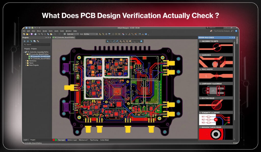
Verification is an essential quality gate before fabrication.
Depending on the rules and tools configured, it can catch:
- Unconnected or incorrectly connected nets
- Clearance violations
- Trace-width violations
- Component placement violations
- Routing-rule violations
- Schematic-to-layout inconsistencies
- Manufacturing-rule conflicts
These checks eliminate a large class of preventable design errors.
But the problem begins when “verification passed” becomes synonymous with “the design is fully validated.”
It isn’t.
A board can satisfy physical and connectivity rules while still having electrical or thermal problems.
Three Problems Verification Can Still Miss
1. High-Speed Signals Can Pass DRC and Still Fail
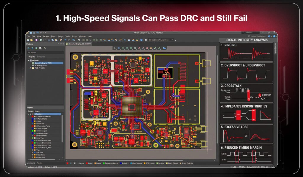
A trace can meet width and spacing requirements and still produce a poor waveform.
Potential problems include:
- Ringing
- Overshoot and undershoot
- Crosstalk
- Impedance discontinuities
- Excessive loss
- Reduced timing margin
Signal behavior depends on the complete interconnect structure, including trace geometry, reference planes, vias, neighbouring signals, and driver/receiver characteristics.
DRC checks the physical rule. SI analysis examines the electrical behavior.
2. A Power Network Can Be Correctly Routed and Still Cause Resets
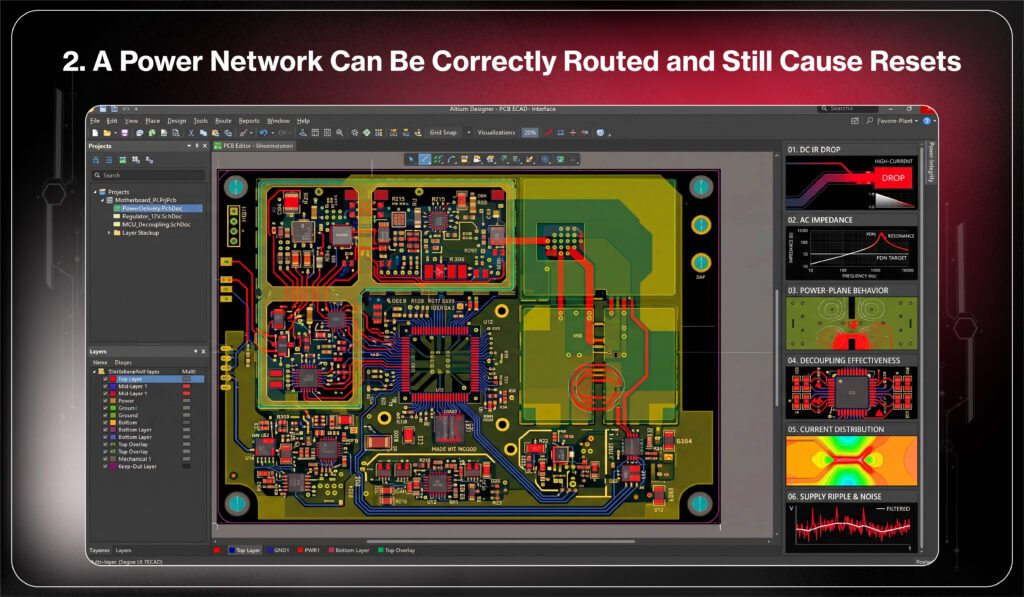
Now consider a processor board.
Connectivity is correct. Power traces meet the required width. Verification passes.
During normal operation, everything appears fine.
Then the processor reaches a high-current workload—and resets.
The investigation may reveal excessive voltage drop, PDN impedance, inadequate decoupling, or power-distribution noise.
Power-integrity analysis can examine:
- DC IR drop
- AC impedance
- Power-plane behavior
- Decoupling effectiveness
- Current distribution
- Supply ripple and noise
The layout did not necessarily violate a rule.
The power network simply did not perform as expected under the actual load.
3. A Correctly Placed Component Can Still Run Too Hot
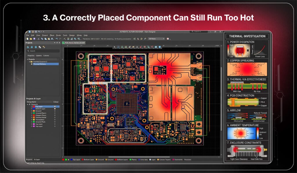
Thermal problems provide another example.
Imagine a power component placed exactly where the layout review requires it. Routing is clean. Clearances pass. Manufacturing rules are satisfied.
But after the board is installed inside its enclosure, the component temperature rises beyond the desired operating range.
Engineers may then need to investigate:
- Power dissipation
- Copper spreading
- Thermal-via effectiveness
- PCB construction
- Airflow
- Ambient temperature
- Enclosure constraints
Physical correctness does not automatically mean thermal adequacy.
Verification vs. Analysis: What Is the Difference?

Verification asks: “Does the PCB meet the defined rules?”
Analysis asks: “Will the PCB perform correctly under real operating conditions?”
Verification checks connectivity, clearances, trace widths, and other design constraints. Analysis goes deeper into signal integrity, power integrity, thermal behavior, impedance, crosstalk, and voltage drop.
Verification catches rule-based errors. Analysis investigates performance risks.
Both are important—especially for high-speed, high-power, and thermally demanding designs.
When Is Verification Not Enough?

Additional analysis becomes especially important for:
- DDR and high-speed memory
- SerDes interfaces
- High-speed processors and FPGAs
- RF or high-frequency circuits
- High-current power sections
- Dense multilayer boards
- Mixed-signal systems
- Thermally constrained products
For these designs, a stronger workflow is:
Schematic → Stackup & DFM Constraints → Layout → Verification → SI Analysis → PI Analysis → Thermal Analysis → DFM Review → Release for Fabrication
But this is not a one-way process.
If SI, PI, thermal, or DFM analysis identifies a problem, the design should loop back to the layout, the issue should be corrected, and verification should be performed again before release.
In practice, the process is closer to:
Design → Verify → Analyze → Correct → Re-verify → Release
The earlier a problem is found, the more options engineers have to correct it.
A trace can be rerouted. A via can be moved. A return path can be improved. Decoupling can be adjusted. Copper distribution can be changed.
After fabrication, those same changes may require board modification or another prototype revision.
Final Answer
Is PCB Design Verification Enough to Prevent Rework?
No—not by itself.
Verification is a necessary quality gate. It can catch connectivity, physical, and rule-based problems before manufacturing.
But it cannot replace analysis of signal integrity, power integrity, thermal behavior, or other performance risks.
The goal is not simply to reach:
“The PCB passed verification.”
It is to reach:
“The major risks that could cause prototype failure have been investigated before fabrication.”
A verified PCB is not necessarily a fully validated PCB.
For complex boards, that difference can mean discovering a problem on the screen rather than discovering it on the prototype.
Verify your PCB beyond basic rules.
Analyze risks before fabrication begins.
Book a Call. Schedule a Free Consultation now. https://calendly.com/gighz/30min
Stuck in a loop of challenges? Always pick smart solution that works
Have you faced costly rework because 2D drawings skipped in MCAD workflows?
Effective way to prevent MCAD documentation errors recalls?
Please answer both poll questions before submitting.
Thank you for your response! 😊
Latest Post
Get Customized Engineering CAD Design Service

Book a Free Consultation Call
Partner with Gighz and bring your most innovative design concepts to life. Our engineering cad services accelerate development so you can focus on your big vision.
