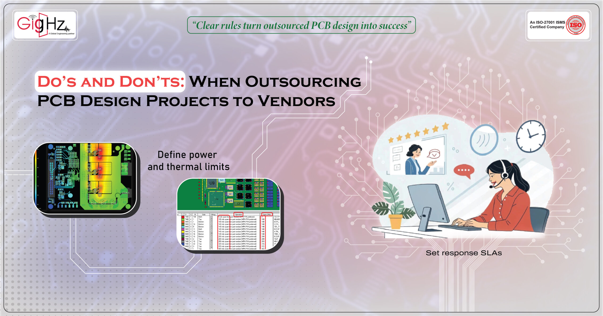
Do’s and Don’ts: When Outsourcing PCB Design Projects
Outsourcing PCB design is not just handing over a schematic and waiting for output.A successful project requires clarity, discipline, and…
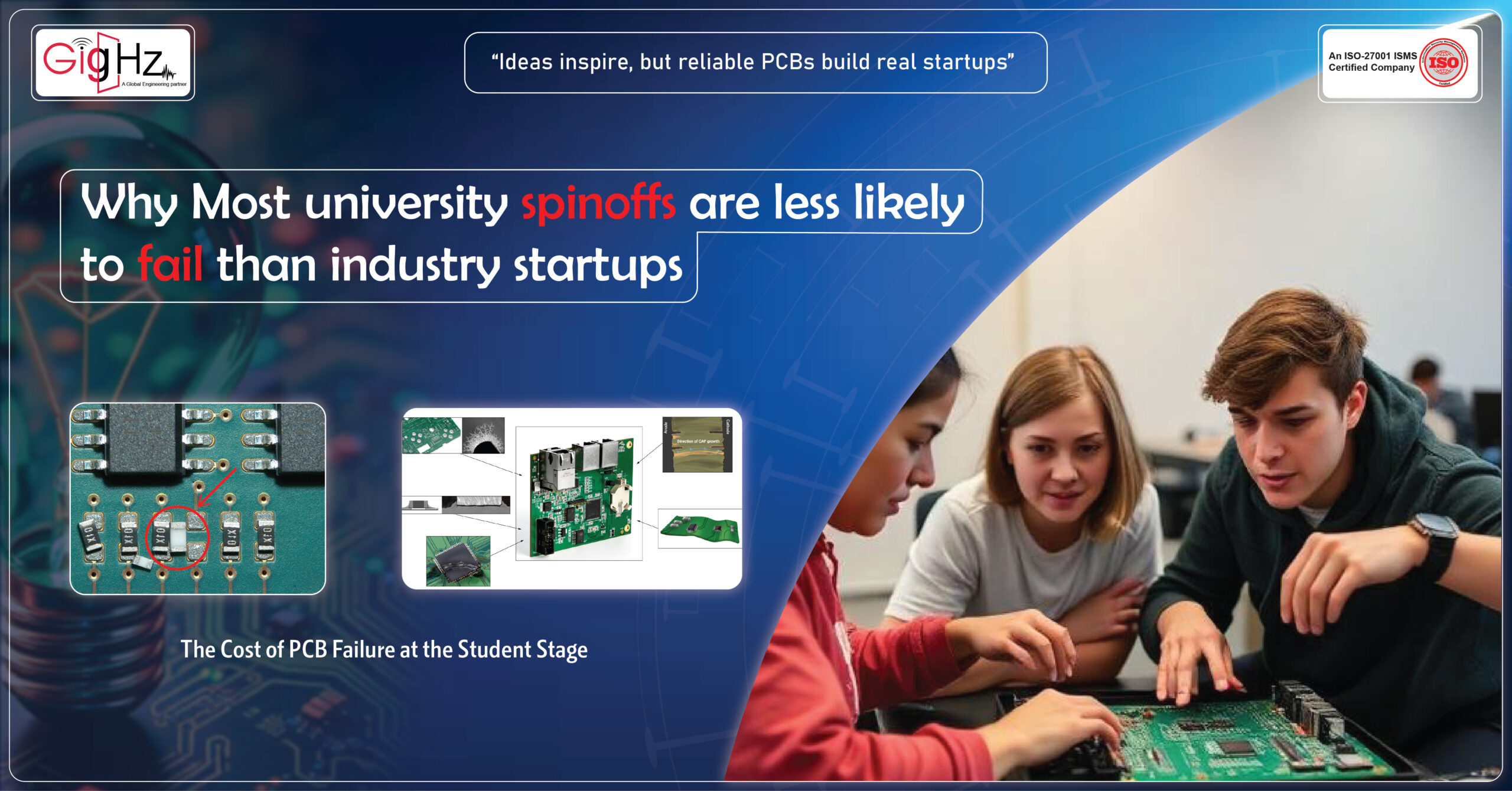
Why Most university spinoffs are less likely to fail than industry startups
Every year, thousands of brilliant ideas are born inside universities. Students win hackathons, build final-year projects, and pitch innovative solutions to…
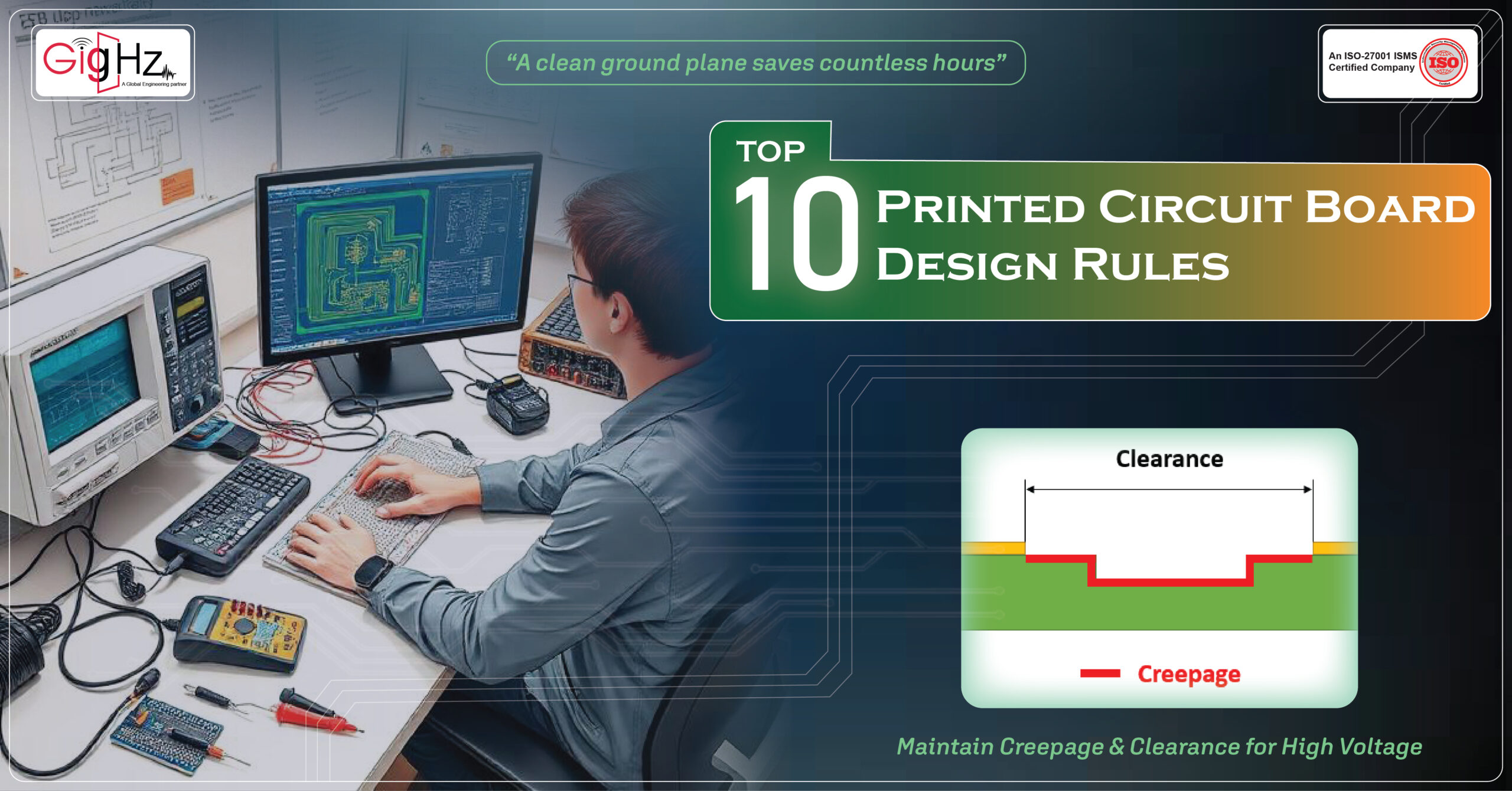
Top 10 Printed Circuit Board Design Rules for Student Hardware Teams
When student hardware teams build their first real printed circuit board design rules, the excitement is high—but so is the…
How to Learn PCB Design: A Simple Guide for University Startups
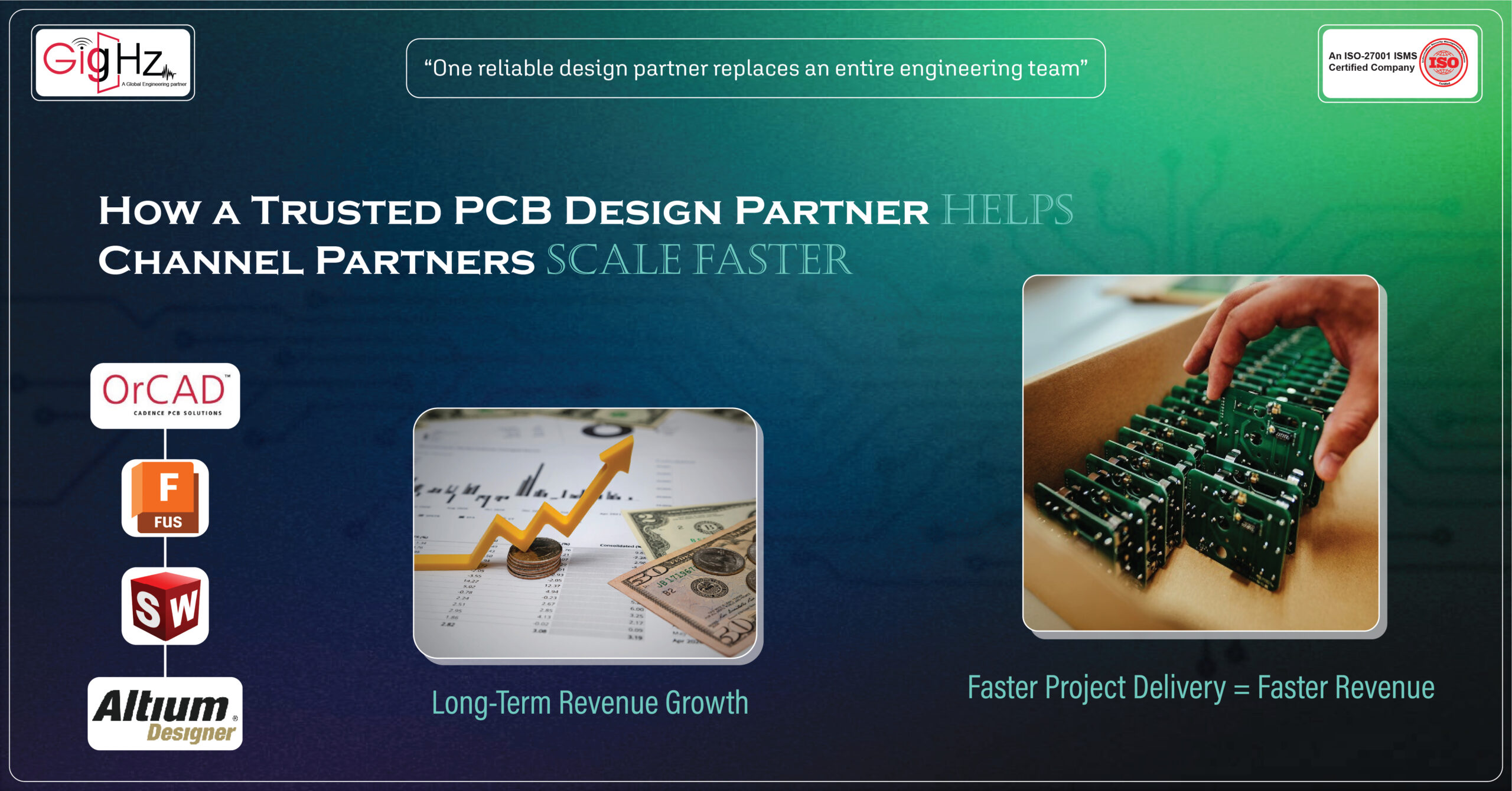
In today’s electronics market, channel partners—distributors, resellers, system integrators, and technology solution providers—are under constant pressure to deliver faster, solve…
How a Trusted PCB Design Partner Helps Channel Partners Scale Faster
In today’s electronics market, channel partners—distributors, resellers, system integrators, and technology solution providers—are under constant pressure to deliver faster, solve…
Do’s and Don’ts: When Outsourcing PCB Design Projects to Vendors
Outsourcing PCB design is not just handing over a schematic and waiting for output.A successful project requires clarity, discipline, and…
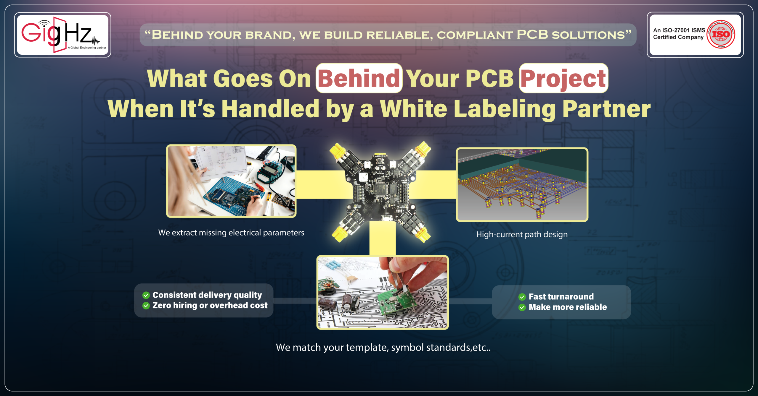
What Goes On Behind Your PCB Project When It’s Handled by a White Labelling Partner
Most agencies, industrial design studios, IoT solution providers, and electronics service companies want to offer PCB design to their clients…

Common Design Mistakes That Slow Down Student-Led Hardware Startup Companies
Every student hardware team knows the excitement of building a new idea. You sketch the system, design the PCB, send…
FAQs University Startups Ask Before Building Their First Prototype
For every university startup, the first prototype isn’t just another project step — it’s the turning point where your idea…
The Real Reason Prototypes Fail Before Investor Demos (for University Teams)
Every university PCB project starts with a working prototype — the LEDs blink, power flows, and the board performs as…
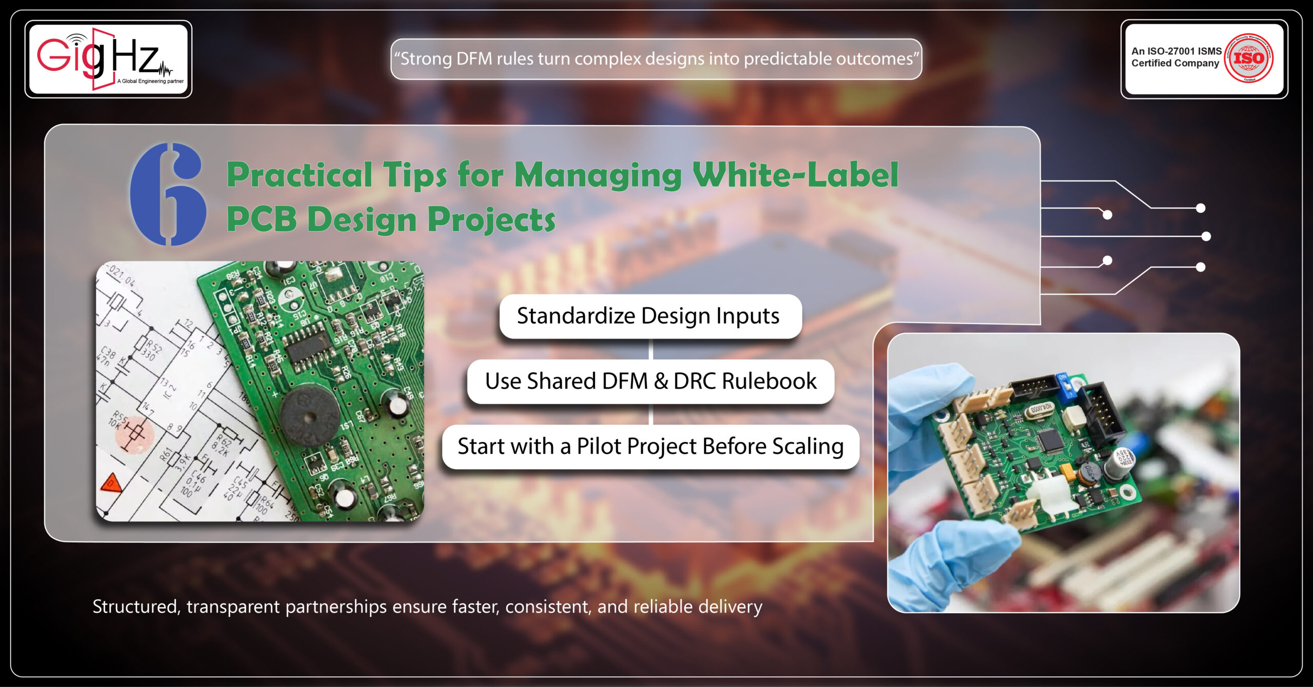
6 Practical Tips for Managing White-Label PCB Design Projects
When you Managing multiple PCB design Projects clients under a white-label model means you’re responsible for both the experience and…
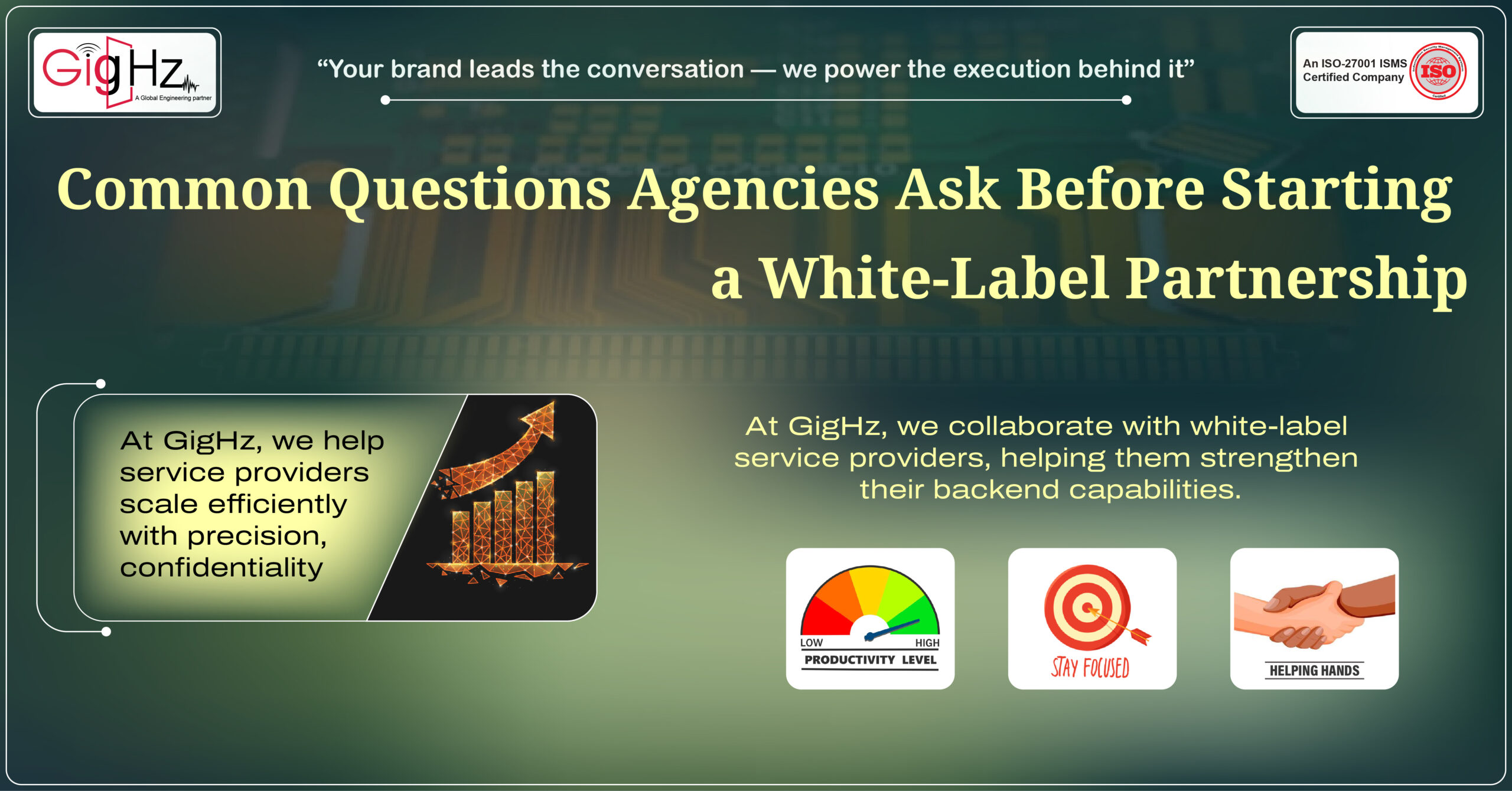
Common Questions Agencies Ask Before Starting a White-Label Partnership
In today’s fast-paced hardware market, white-label Partnership face increasing pressure to deliver complete product solutions — from concept to production…