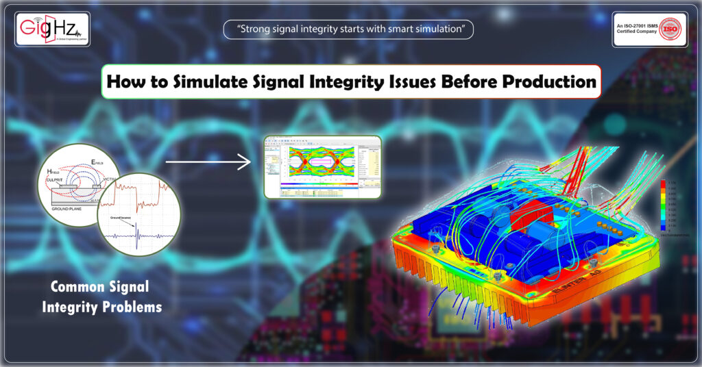
How to Simulate Signal Integrity Issues Before Production
- Posted On:
- December 12, 2025
- Category:
- Analysis & Simulation
Every PCB designer wants one thing — a board that works perfectly the very first time it’s powered on.
But reality often tells a different story. You complete the schematic, follow every layout rule, and still, when the prototype arrives, something feels off.
Signals glitch. Timing fails. Noise creeps in where it shouldn’t.
That’s the world of signal integrity issues — a world that doesn’t show up on the schematic but decides whether your design succeeds or fails.
And once the board is fabricated, discovering signal problems can be painful and costly.
That’s why today’s smart PCB designers don’t wait for lab results to tell them what went wrong.
They simulate signal integrity issues before production — when every problem is still fixable and every correction is just a few clicks away.
In this blog, let’s explore how you can understand, simulate, and prevent signal integrity failures before your board ever reaches the manufacturer.
We’ll break it down step by step — from common problems to the tools, methods, and design practices that make your signal behavior predictable and reliable.
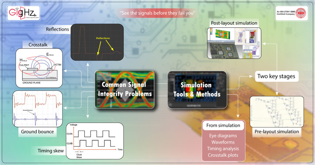
1. Common Signal Integrity Problems
Before you can fix something, you need to see how it breaks.
Signal integrity (SI) problems come from one simple fact: high-speed signals behave like waves, not just voltage lines.
When signal edges get faster (below 1 ns rise time) or frequencies exceed 50 MHz, those signals start to act like transmission lines.
That means reflections, ringing, and delay can appear even if the frequency isn’t “that high.”
Here are some common SI issues that can quietly destroy performance:
- Reflections: When the trace impedance doesn’t match the load, part of the signal bounces back. This causes overshoot or undershoot, which distorts logic levels.
- Crosstalk: When nearby traces are too close, one signal couples into another, creating noise that shifts timing or triggers false logic.
- Ground bounce: Fast switching of multiple outputs causes voltage fluctuations in the ground plane.
- Timing skew: Signals that should arrive together reach at slightly different times, causing setup or hold violations.
In the early stages, these problems don’t show up in schematics.
But once you simulate, you start seeing the real behavior of your design — how traces talk to each other, how vias add delay, and how return paths shape the waveform.
2. Simulation Tools & Methods
Simulation is like having an x-ray for your PCB — it lets you see what’s happening inside your traces before manufacturing.
And there are two key stages where you can simulate signal integrity: pre-layout and post-layout.
Pre-layout simulation happens before routing begins.
Here, you define models of your components, estimate trace lengths, and check expected rise times.
This helps you plan the layer stack, impedance targets, and termination strategies early — so your layout starts right.
Post-layout simulation happens after routing is complete.
This is where the tool analyzes your actual design — trace geometries, via structures, coupling, and termination networks — and shows real signal waveforms.
Modern tools like Mentor HyperLynx, Cadence Sigrity, and Ansys SIwave allow you to run both stages smoothly.
They use IBIS or SPICE models to simulate signal transitions and visualize voltage levels over time.
Through simulation, you can view:
- Eye diagrams to check data quality and timing margin.
- Waveforms to identify ringing or distortion.
- Timing analysis to detect skew or delay mismatches.
- Crosstalk plots to locate coupling hotspots.
When you see a distorted signal in simulation, it’s not a failure — it’s a warning.
It gives you a chance to correct trace impedance, adjust spacing, or modify termination resistors before a single PCB is made.
That’s the power of simulation — it replaces uncertainty with insight.
3. Impedance & Crosstalk Control
Two of the biggest culprits behind signal integrity failures are impedance mismatch and crosstalk.
Simulation helps you see both clearly.
Let’s start with impedance control.
Every trace in your PCB behaves like a transmission line with a characteristic impedance — often 50 Ω for single-ended and 90 Ω for differential pairs.
If your trace impedance doesn’t match the driver and receiver, part of the signal reflects back.
This is what creates overshoot, undershoot, or ringing.
Simulation tools calculate impedance based on trace width, dielectric thickness, copper thickness, and dielectric constant.
By adjusting these parameters, you can reach the exact impedance value your design needs.
Now, on to crosstalk.
When two high-speed traces run in parallel too closely, their electromagnetic fields overlap.
This coupling transfers noise from one trace to another — called near-end and far-end crosstalk.
During simulation, you can view crosstalk coupling coefficients and see how much one net affects another.
By increasing spacing, adding ground shields, or re-routing traces on different layers, you can drastically reduce this unwanted interaction.
It’s amazing how simulation can visually confirm something you might only guess otherwise.
You can literally see how a 2 mm spacing change drops crosstalk by half.
It’s not just theory — it’s engineering made visible.
4. Preventing SI Failures Before They Happen
The ultimate goal of signal integrity simulation isn’t just to find issues — it’s to build confidence in your design.
Once you’ve simulated and seen the waveform quality, you can start refining your design parameters:
- Routing adjustments: Shorter routes for critical signals, smoother transitions, and controlled layer changes.
- Termination tuning: Adjusting resistor values to reduce reflections.
- Stackup optimization: Choosing the right dielectric and layer order to maintain return paths.
- Via optimization: Reducing stubs or using back-drilling for high-speed layers.
Each of these steps fine-tunes your board for real-world behavior.
Another big advantage is design reuse. Once you’ve validated a signal interface through simulation — say DDR4 or USB 3.0 — you can reuse those models in future projects with confidence.
That saves both time and effort for your next design.
Most importantly, simulation helps avoid the validation risk of prototype failure.
Instead of worrying about what might go wrong, you already know what’s stable and what’s risky.
You no longer rely only on experience or assumptions — you have proof, visual and measurable.
Bottom Line
In PCB design, uncertainty is expensive.
A single overlooked signal integrity issue can delay production, waste prototypes, and damage your company’s reputation.
But when you simulate signal integrity issues before production, you turn that uncertainty into control.
You see how signals behave, you understand what causes distortion, and you fix it before it becomes a costly problem.
Signal integrity isn’t just a technical concern — it’s about confidence.
It’s about knowing your design will work the first time it’s powered on.
And that’s what great engineering is all about — solving problems before they even exist.
Book a Call. Schedule a Free Consultation https://calendly.com/gighz/30min
Stuck in a loop of challenges? Always pick smart solution that works
Have you faced costly rework because 2D drawings skipped in MCAD workflows?
Effective way to prevent MCAD documentation errors recalls?
Please answer both poll questions before submitting.
Thank you for your response! 😊
Latest Post
Get Customized Engineering CAD Design Service

Book a Free Consultation Call
Partner with Gighz and bring your most innovative design concepts to life. Our engineering cad services accelerate development so you can focus on your big vision.