

PCB Design Review Passed—Can SI/PI Reveal Hidden Issues?
- Posted On:
- November 18, 2026
- Category:
- Ecad, Analysis & Simulation

A PCB can pass every design check and still leave one critical question unanswered: will it actually perform?
DRC may be clean, routing constraints may be satisfied, and the design review may be complete. Yet impedance discontinuities, crosstalk, return-path issues, voltage droop, or PDN resonance can remain hidden until the board operates at real switching speeds and load conditions.
That is why PCB Design Review alone cannot tell the complete electrical story. SI/PI analysis goes deeper, revealing how critical signals and power networks are likely to behave before those hidden issues turn into prototype failures.
What a PCB Design Review Can Confirm—and What It Cannot
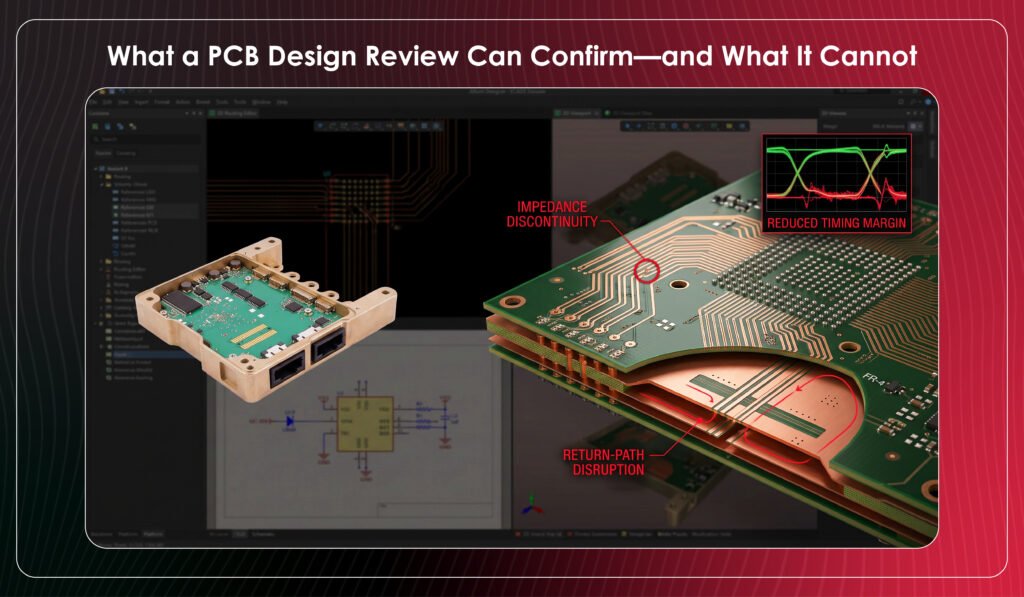
A design review can confirm that the PCB follows physical, routing, connectivity, and manufacturing rules.
But these checks do not always reveal how the board will behave electrically.
A differential pair may meet its length and spacing constraints while a BGA escape creates an impedance discontinuity. A connector can also change channel characteristics.
A plane interruption can force return current onto a longer path.
For example, a DDR interface can satisfy length-matching requirements but still lose timing margin because of reflections introduced by vias, packages, or interconnect discontinuities.
The design may be technically compliant, but its electrical margin can still be inadequate.
How SI Analysis Uncovers Hidden Signal Risks

At fast edge rates, a PCB trace behaves as a transmission structure rather than an ideal wire.
Trace geometry, dielectric properties, vias, connectors, package parasitics, and termination all influence the signal reaching the receiver.
Signal Integrity (SI) analysis can evaluate:
- Impedance variation
- Reflections and ringing
- Overshoot and undershoot
- Crosstalk
- Propagation delay
- Insertion and return loss
- Eye height and eye width
- Jitter and voltage margin
- Via and connector discontinuities
Consider a high-speed signal changing layer through a via field.
The routing may pass length, clearance, and spacing checks, but the via transition can still disturb impedance. Post-layout SI analysis can use the actual routed interconnect to determine whether that discontinuity affects the receiver waveform.
Instead of simply seeing a noisy waveform, engineers can identify measurable effects such as reduced eye opening, increased jitter, or excessive reflection.
That turns a prototype symptom into an engineering problem that can be investigated and corrected.
How Return-Path Issues Connect Signal and Power Integrity
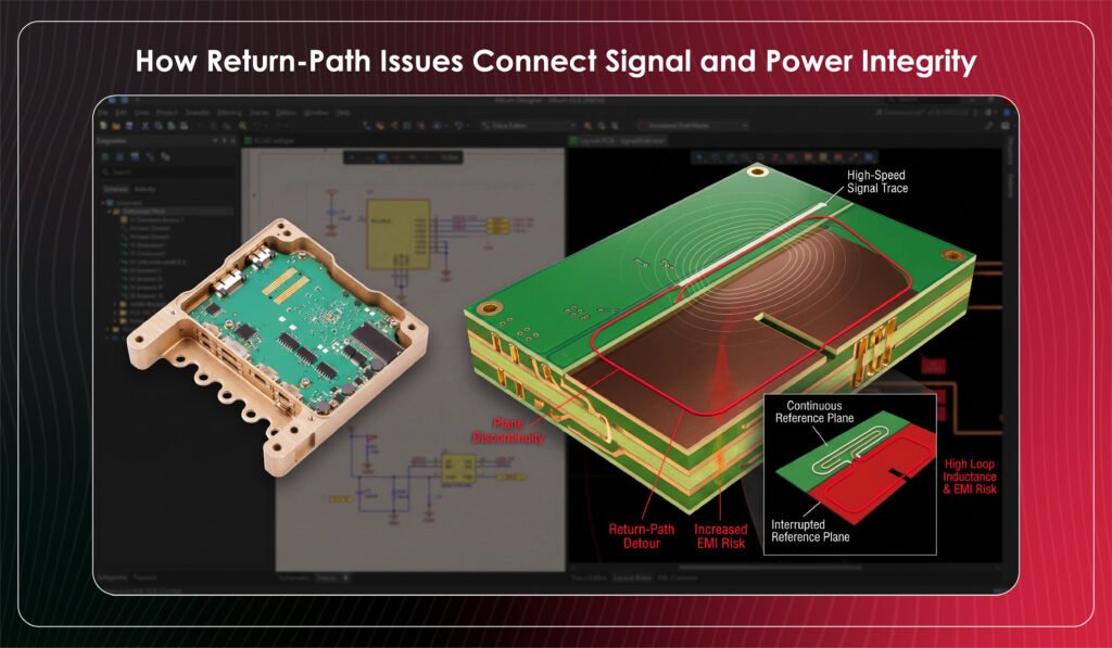
At high frequencies, return current tends to follow the reference plane closest to the signal.
If that path is interrupted by a split, slot, void, or unsuitable layer transition, current must find another route.
That increases loop inductance and can increase coupling and EMI risk.
A high-speed trace can therefore meet every routing rule and still have a poor return path.
The practical check is straightforward: maintain continuous reference planes beneath critical signals and avoid transitions that unexpectedly force return current around obstacles.
SI analysis can then help quantify the electrical impact of the physical structure.
What PI Analysis Reveals Under Load

Power Integrity (PI) problems often appear when current demand changes quickly—not while the board is idle.
A processor may reset during a workload. An FPGA may become unstable during simultaneous switching. An ADC may show increased noise when another device changes operating state.
The schematic can contain the correct regulators and capacitors while the physical power delivery network (PDN) still performs poorly.
PI analysis can examine:
- PDN impedance
- Voltage drop
- Resonance and anti-resonance
- Decoupling effectiveness
- Load-transient response
- Power-plane behavior
Real components are not ideal. Capacitor ESR and ESL, package parasitics, mounting inductance, vias, plane geometry, and load transients all influence the power network.
A frequency-domain impedance plot can expose a resonance peak that may be difficult to identify from the schematic alone.
SI/PI Problems to Catch Before Fabrication
1. A Via Transition Creates Ringing
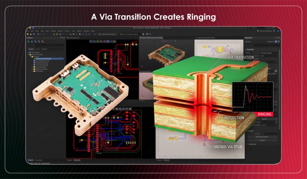
A high-speed net meets routing constraints, but its via structure creates an impedance discontinuity.
Possible result: reflections and ringing reduce receiver voltage or timing margin.
2. Coupled Signals Reduce Noise Margin
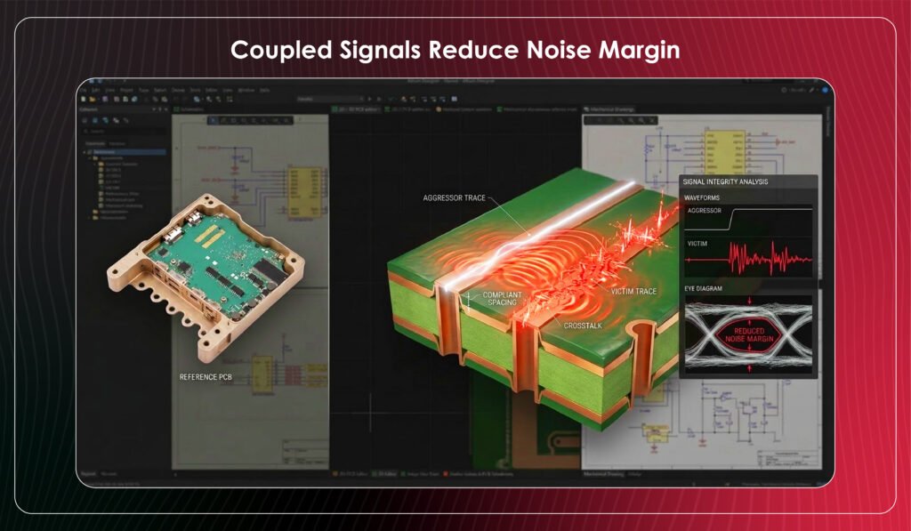
Two fast signals satisfy the defined spacing rule, but their edge rates and parallel routing produce unwanted coupling.
Possible result: crosstalk reduces signal margin or contributes to eye closure.
3. A PDN Resonance Appears During Load Changes
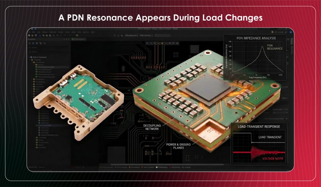
The power network contains correctly selected capacitors, but component and layout parasitics create an impedance peak at a critical frequency.
Possible result: transient voltage noise contributes to processor, FPGA, or converter instability.
These scenarios show why electrical validation adds another layer of confidence beyond physical design checks.
Use SI/PI Before and After Layout
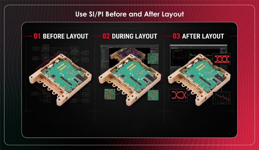
SI/PI analysis is most useful when it supports decisions throughout the design cycle.
Before layout:
- Establish impedance targets
- Identify critical interfaces
- Define topology and termination strategy
- Set power-delivery targets
During layout:
- Control BGA breakout and via transitions
- Maintain reference-plane continuity
- Manage differential routing
- Position decoupling capacitors effectively
After layout:
- Analyze actual traces and vias
- Evaluate signal waveforms
- Check channel and PDN behavior
- Investigate electrical margins
The goal is not to simulate every net.
It is to identify the signals and power networks most likely to create expensive hardware problems
Final Answer
A successful PCB Design Review confirms that the board meets its physical, connectivity, routing, and manufacturing requirements.
But passing those checks does not guarantee how critical signals and power networks will behave under real operating conditions.
That is where SI/PI analysis adds another layer of confidence. It can reveal reflections, crosstalk, return-path disruption, eye-margin loss, PDN resonance, and voltage droop before they become costly prototype problems.
The real question is not just “Did the board pass review?”
It is “Will it perform as intended?”
Passing DRC proves design-rule compliance. SI/PI analysis helps turn a compliant layout into a more predictable, reliable prototype.
Catch hidden SI/PI risks before fabrication.
Validate your critical signals and power networks.
Book a Call. Schedule a Free Consultation now. https://calendly.com/gighz/30min
Stuck in a loop of challenges? Always pick smart solution that works
Have you faced costly rework because 2D drawings skipped in MCAD workflows?
Effective way to prevent MCAD documentation errors recalls?
Please answer both poll questions before submitting.
Thank you for your response! 😊
Latest Post
Get Customized Engineering CAD Design Service
Book a Free Consultation Call
Partner with Gighz and bring your most innovative design concepts to life. Our engineering cad services accelerate development so you can focus on your big vision.
