

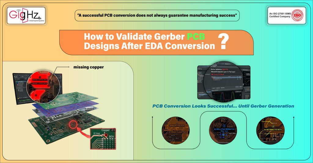
The PCB conversion looks successful at first glance.
Files import correctly, and the layout opens without warnings.
But issues often show up after Gerber generation in modern Gerber PCB designs.
During fabrication review, unexpected problems can appear—missing copper, broken polygons, drill mismatches, shifted pads, or connectivity errors that were never visible in the design tool.
In some cases, the prototype powers on but fails during bring-up due to hidden conversion issues in the manufacturing data.
These problems are difficult to catch because the board still looks correct visually. The issues exist inside the output files used for fabrication and only become visible later during production or testing.
For university spin-offs and product engineering teams, even a small unnoticed Gerber issue can delay prototypes, increase costs, and slow down development.
That’s why EDA conversion is not just about opening a design in another tool—it’s about ensuring the manufacturing output is still fully correct and reliable after conversion.
Why Gerber Validation Matters After EDA Conversion
EDA conversion changes how design data is interpreted between different software environments.
Even when the schematic and layout appear visually correct, small translation inconsistencies can affect manufacturing outputs.
“In high-speed and multi-layer Gerber PCB design projects, even small translation inconsistencies can create manufacturing risks.”
These issues may include:
- Layer mapping errors
- Missing copper regions
- Incorrect drill alignment
- Broken polygons
- Aperture mismatches
- Net connectivity problems
- Solder mask inconsistencies
Many of these problems do not appear during normal layout review. They become visible only after Gerber generation or during fabrication.
This is why post-conversion validation is essential before releasing data for manufacturing.
Key Areas to Validate After EDA Conversion
1. Verify Layer Mapping Accuracy
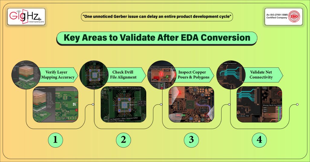
One of the most common conversion issues involves incorrect layer translation between EDA tools.
Always confirm:
- Copper layers are assigned correctly
- Silkscreen layers are intact
- Solder mask openings are accurate
- Mechanical and drill layers match the original design intent
Even a small layer mismatch can create fabrication errors.
2. Check Drill File Alignment
Drill data must align perfectly with pads and vias.
Validate:
- Through-hole alignment
- Via positioning
- Drill sizes
- Annular ring integrity
Misaligned drill files can cause open circuits or unreliable connections during manufacturing.
3. Inspect Copper Pours and Polygons
Polygon conversion issues are common after EDA migration.
Carefully inspect:
- Ground pours
- Copper islands
- Plane clearances
- Thermal relief connections
Broken copper regions may not appear obvious visually but can affect grounding, power integrity, and manufacturability.
4. Validate Net Connectivity
A design may appear connected graphically while electrical connectivity is partially broken internally.
Check for:
- Disconnected traces
- Missing vias
- Broken power nets
- Floating copper sections
Run connectivity verification before releasing Gerbers.
5. Review Apertures and Trace Geometry
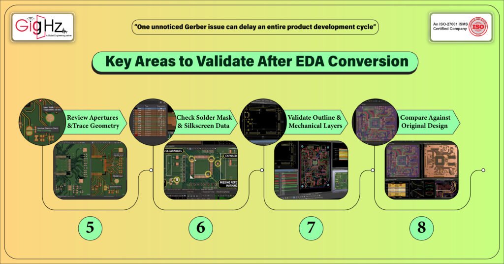
Gerber generation depends heavily on aperture interpretation.
Verify:
- Trace widths
- Pad dimensions
- Shape consistency
- Fine-pitch feature accuracy
Incorrect aperture translation can distort manufacturing geometry.
6. Check Solder Mask and Silkscreen Data
Solder mask and silkscreen issues often appear after format translation.
Inspect:
- Mask clearances
- Exposed pads
- Silkscreen overlap
- Missing reference markings
These issues directly affect assembly quality and inspection.
7. Validate Board Outline and Mechanical Layers
Mechanical layer inconsistencies can create manufacturing confusion.
Confirm:
- Board dimensions
- Slot definitions
- Cutouts
- Edge routing data
Incorrect mechanical data can delay fabrication or assembly preparation.
8. Compare Against Original Design Intent
Validation is not only about checking Gerber files individually.
It is about confirming the converted outputs still match the original engineering intent.
Compare:
- Stack-up structure
- Critical routing regions
- Controlled impedance paths
- Differential pair geometry
- High-speed routing sections
Small conversion changes can affect electrical behavior even when layouts appear visually similar.
Common Mistakes Teams Miss
This creates risk because some issues remain electrically hidden.
Commonly missed problems include:
- Broken return paths
- Corrupted polygon connections
- Unintended clearance changes
- Layer polarity inversion
- Missing thermal reliefs
- Incorrect drill mapping
These issues often appear only during fabrication or board bring-up.
Why This Matters for University Spinoffs
For university hardware teams and emerging product companies, PCB prototypes are directly connected to:
- Research validation
- Investor demonstrations
- Product testing timelines
- Commercialization milestones
A hidden Gerber issue can delay an entire development cycle.
That is why Gerber validation after EDA conversion should be treated as a manufacturing risk-control process—not just a file export step.
Final Thought
EDA conversion is not complete when the design opens successfully in a new tool.
It is complete only when the manufacturing outputs are fully validated.
In any Gerber PCB design, Gerber files represent the final physical interpretation of the layout before fabrication.
If hidden conversion issues remain inside these outputs, they can affect fabrication, assembly, performance, and prototype reliability.
By validating layer mapping, drill data, copper integrity, connectivity, and manufacturing geometry early, engineering teams can reduce redesign cycles, improve manufacturing confidence, and protect product development timelines.
For modern hardware development, Gerber validation is not just a technical review—it is a critical step in ensuring reliable product execution.
Want to avoid hidden issues in your design?
Connect with us for the expert free consultation
https://calendly.com/gighz/30min
Stuck in a loop of challenges? Always pick smart solution that works
Have you faced costly rework because 2D drawings skipped in MCAD workflows?
Effective way to prevent MCAD documentation errors recalls?
Please answer both poll questions before submitting.
Thank you for your response! 😊
Latest Post
Get Customized Engineering CAD Design Service

Book a Free Consultation Call
Partner with Gighz and bring your most innovative design concepts to life. Our engineering cad services accelerate development so you can focus on your big vision.
