

How to Fix Hidden PCB Design Issues That Affect Signal Integrity
- Posted On:
- September 28, 2026
- Category:
- Ecad
You completed the schematic.
The layout looks clean.
DRC passes without major violations.
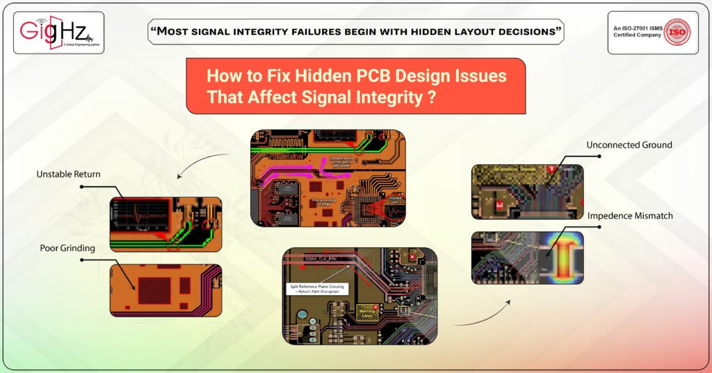
But during testing, the board still shows unexpected noise, timing instability, EMI issues, or unreliable high-speed performance.
These PCB design issues are some of the most frustrating problems engineers face during hardware validation.
Because in many cases, the failure is not caused by the circuit itself—it is caused by hidden layout-level signal integrity issues that were never visible during initial design checks.
A small impedance discontinuity, an unstable return path, poor grounding strategy, via discontinuities, or unwanted coupling between traces can quietly affect signal behavior long before the problem becomes visible during validation.
That is why high-speed PCB design is no longer just about routing connections. It is about controlling how signals physically behave across the board under real operating conditions.
9 Hidden PCB Design Issues and How to Fix Them
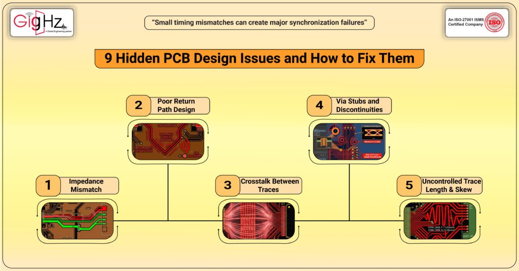
1. Impedance Mismatch
When impedance changes along a signal path, part of the signal energy reflects back toward the source instead of continuing smoothly to the receiver.
This creates signal distortion, ringing, overshoot, undershoot, and timing instability.
Impedance mismatch commonly occurs due to:
- Sudden trace width changes
- Inconsistent stack-up structure
- Improper via transitions
- Reference plane discontinuities
- Connector and pad geometry changes
At high edge rates, even small impedance discontinuities can significantly affect signal quality.
How to Fix It
- Use controlled impedance routing
- Maintain consistent trace width
- Define stack-up before routing begins
- Avoid abrupt geometry changes
- Validate impedance with fabrication constraints
A stable impedance path improves signal integrity and reduces reflections.
2. Poor Return Path Design
A signal path is always a complete current loop consisting of:
- Forward current path
- Return current path
At high frequencies, return current follows the path of lowest impedance directly beneath the signal trace through the reference plane.
When return paths are interrupted by:
- Split planes
- Gaps in ground
- Poor layer transitions
- Broken reference structures
the current is forced to spread outward, increasing loop area, EMI radiation, and noise coupling.
How to Fix It
- Maintain continuous ground planes
- Avoid routing across split planes
- Keep reference planes directly below high-speed signals
- Add stitching vias near signal transitions
Good return path continuity is critical for stable high-speed performance.
3. Crosstalk Between Traces
Closely spaced traces create capacitive and inductive coupling between adjacent signals.
This unwanted coupling transfers energy from one trace to another and creates noise interference.
Crosstalk becomes more severe when:
- Parallel routing distance increases
- Trace spacing decreases
- Edge rates become faster
- Return paths are poorly controlled
This can lead to:
- False switching
- Signal corruption
- Reduced timing margins
How to Fix It
- Increase spacing between high-speed traces
- Reduce long parallel routing sections
- Route sensitive signals away from noisy nets
- Use grounded shielding where required
- Keep signals close to their reference planes
Proper spacing and field containment reduce coupling effects.
4. Via Stubs and Discontinuities
Vias introduce parasitic inductance and capacitance into signal paths.
Unused via barrel sections create via stubs, which behave like resonant structures at high frequencies.
These discontinuities cause:
- Signal reflections
- Increased insertion loss
- Resonance effects
- Reduced eye diagram quality
Via-related issues often become critical in:
- DDR interfaces
- PCIe
- SerDes
- RF layouts
How to Fix It
- Minimize unnecessary layer transitions
- Use back-drilling for high-speed vias
- Consider blind or buried vias
- Keep via structures consistent across critical nets
Reducing discontinuities improves signal continuity.
5. Uncontrolled Trace Length and Skew
High-speed interfaces rely on precise timing relationships between signals.
When electrical delays vary between traces, skew occurs.
This leads to:
- Timing errors
- Synchronization failures
- Reduced setup and hold margins
- Data corruption
Physical trace length alone does not define timing.
Delay also depends on:
- Dielectric properties
- Layer structure
- Routing geometry
How to Fix It
- Match electrical delays on timing-critical nets
- Route differential pairs symmetrically
- Use tuning only where necessary
- Avoid excessive serpentine routing
Accurate delay matching improves timing reliability.
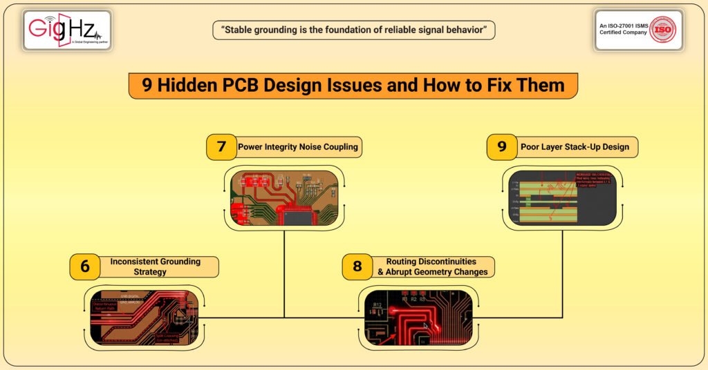
6. Inconsistent Grounding Strategy
Ground planes provide:
- Signal reference
- Return current path
- EMI control
- Reference stability
Fragmented or poorly connected grounding structures create unstable reference behavior and increase noise susceptibility.
Common problems include:
- Split grounds without proper control
- Floating copper regions
- Poor via stitching
- Long return current detours
How to Fix It
- Use solid continuous ground planes
- Maintain proper ground stitching
- Avoid unnecessary plane splits
- Keep high-speed return paths short and direct
Stable grounding improves both SI and EMI performance.
7. Power Integrity Noise Coupling
Signal integrity and power integrity are directly connected.
Noise in the Power Distribution Network (PDN) changes voltage reference stability and introduces noise into signal paths.
Poor PDN behavior causes:
- Voltage ripple
- Ground bounce
- Switching noise
- Jitter in high-speed signals
This often occurs when:
- Decoupling is poorly placed
- Power impedance is too high
- Return paths are weak
How to Fix It
- Place decoupling capacitors close to IC power pins
- Maintain low PDN impedance
- Use solid power and ground planes
- Minimize loop area in power delivery paths
Stable power delivery improves overall signal quality.
8. Routing Discontinuities and Abrupt Geometry Changes
Sudden routing geometry changes disturb electromagnetic field distribution along the trace.
Examples include:
- Sharp bends
- Neck-down routing
- Sudden width transitions
- Poorly optimized pad entries
These discontinuities introduce localized impedance variation and increase reflections in very high-speed designs.
How to Fix It
- Maintain smooth routing geometry
- Use gradual transitions where possible
- Avoid unnecessary width changes
- Maintain consistent routing structures
Uniform geometry improves impedance continuity.
9. Poor Layer Stack-Up Design
Layer stack-up controls:
- Impedance behavior
- Return path quality
- EMI containment
- Crosstalk performance
- Power integrity
Poor stack-up planning creates unstable electrical behavior even when routing appears correct.
Common stack-up problems include:
- Large signal-to-plane spacing
- Weak plane coupling
- Improper layer pairing
- Inconsistent dielectric thickness
How to Fix It
- Define stack-up before layout begins
- Keep signal layers adjacent to reference planes
- Maintain proper dielectric control
- Coordinate stack-up with fabrication capabilities
A well-structured stack-up forms the foundation of stable PCB performance.
How These Issues Affect Real Designs
These issues rarely appear in isolation. They interact with each other and create complex problems.
For example, a small impedance mismatch may not cause immediate failure. But when combined with poor return paths and crosstalk, it can lead to significant signal degradation.
Similarly, power noise may seem manageable on its own. But when combined with grounding issues and routing discontinuities, it can create unstable system behavior.
This interaction is what makes signal integrity problems difficult to diagnose. The root cause is often not a single issue, but a combination of multiple small design decisions.
Final Thought
Hidden design issues are one of the main reasons PCB design issues appear late in development.
They do not show up during initial checks, but they directly affect performance, reliability, and manufacturability.
The solution is not just fixing issues after they appear. It is designing in a way that prevents them from occurring in the first place.
By controlling impedance, maintaining proper return paths, managing routing carefully, and validating decisions early, most signal integrity problems can be avoided.
Strong design practices lead to stable performance, fewer iterations, and more reliable products.
Want to avoid hidden issues in your design?
Connect with us for the expert free consultation
https://calendly.com/gighz/30min
Stuck in a loop of challenges? Always pick smart solution that works
Have you faced costly rework because 2D drawings skipped in MCAD workflows?
Effective way to prevent MCAD documentation errors recalls?
Please answer both poll questions before submitting.
Thank you for your response! 😊
Latest Post
Get Customized Engineering CAD Design Service

Book a Free Consultation Call
Partner with Gighz and bring your most innovative design concepts to life. Our engineering cad services accelerate development so you can focus on your big vision.
