

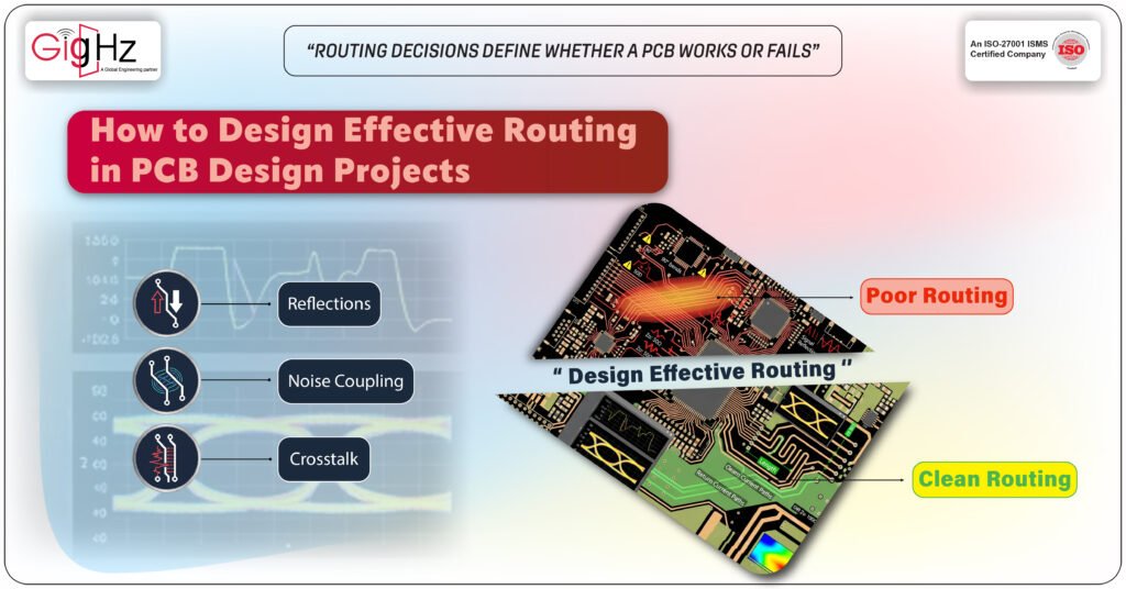
In PCB design, routing is where theory meets reality.
Routing in PCB design defines how signals behave in real-world conditions.
You can have a perfect schematic, carefully selected components, and validated simulations—but if routing is not done correctly, the board will still fail in real-world conditions.
Many designers assume routing is simply about connecting points. In simpler or lower-speed designs, basic routing may appear sufficient initially, but layout quality still affects reliability and noise performance.
But as signal speeds increase and layouts become denser, routing decisions start to directly affect signal integrity, EMI behavior, timing accuracy, and overall system stability.
In real-world PCB design, routing is not just about connections—it is about controlling how signals behave as they travel across the board.
Even small mistakes in routing can lead to reflections, noise coupling, crosstalk, and unpredictable system behavior.
That is why understanding effective routing practices is essential for building reliable and high-performance PCBs.
What Effective Routing Really Means
Effective routing ensures signal paths maintain electrical integrity while meeting physical constraints.
It involves:
- Signal integrity
- Impedance control
- Return paths
- Crosstalk
- Timing
At high frequencies, traces act like transmission lines, so routing choices directly affect signal behavior.
Poor routing leads to noise and instability, while good routing ensures reliable performance.
Key Principles for Routing in PCB Design
Improving routing quality does not require complex tools alone.
It requires discipline, planning, and an understanding of signal behavior.
Let’s break down the most important routing practices.
1. Always Route Over a Continuous Ground Plane
A solid ground plane is essential for maintaining signal integrity.
At high frequencies, return current typically follows the lowest impedance path directly beneath the signal trace.
If the ground plane is broken or split, the return path is disrupted, leading to increased noise and EMI.
Best practices:
- Keep ground planes continuous
- Avoid routing signals across split planes
- Ensure a clear return path under every signal
A stable return path ensures consistent signal behavior and reduces interference.
2. Maintain Controlled Impedance
At high speeds, traces must be designed with controlled impedance to prevent reflections.
To achieve this:
- Maintain consistent trace width
- Control dielectric thickness
- Keep spacing uniform for differential pairs
Sudden changes in trace geometry cause impedance mismatches, which result in signal reflections and distortion.
Consistent impedance ensures smooth signal transmission across the board.
3. Minimize Via Usage in Critical Paths
Vias introduce parasitic inductance and capacitance, which affect signal quality.
While vias are necessary, excessive usage in high-speed paths can degrade performance.
Guidelines:
- Keep signal paths as direct as possible
- Avoid unnecessary layer transitions
- Use optimized via structures when needed
Reducing vias improves signal continuity and minimizes unwanted effects.
4. Control Trace Length and Delay Matching
In high-speed systems, timing is critical.
Signals that arrive at different times can cause data errors and synchronization issues. This is especially important for interfaces like DDR, PCIe, and high-speed buses.
To manage this:
- Match lengths of critical signal paths
- Use serpentine routing where needed
- Focus on delay matching, not just physical length
Accurate timing ensures reliable communication between components.
5. Maintain Proper Trace Spacing
Closely spaced traces can couple noise into each other, leading to crosstalk.
To reduce interference:
- Increase spacing between high-speed signals
- Avoid long parallel routing of sensitive traces
- Separate noisy and sensitive signal paths
Proper spacing helps maintain clean signal waveforms and reduces errors.
6. Route Differential Pairs Carefully
Differential signals rely on symmetry for proper operation.
Any imbalance between the pair can introduce noise and timing issues.
Best practices:
- Keep equal trace lengths
- Maintain consistent spacing
- Route both traces together on the same layer
Symmetrical routing ensures that differential signals remain balanced and stable.
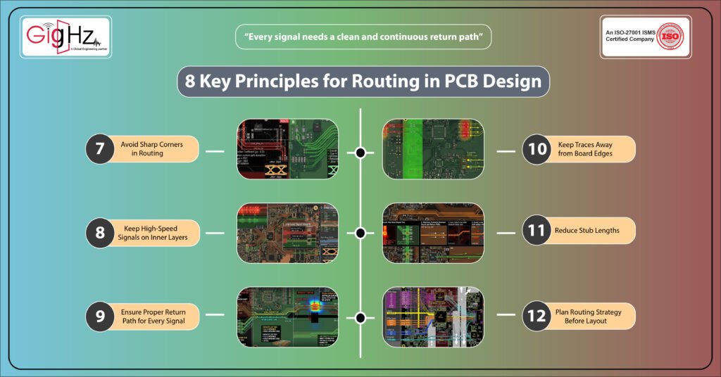
7. Avoid Sharp Corners in Routing
Sharp angles in traces can cause impedance discontinuities and signal reflections.
Instead of 90-degree bends, use:
- 45-degree angles
- Smooth curved routing
This maintains uniform impedance and improves signal quality.
8. Keep High-Speed Signals on Inner Layers
Inner layers provide better shielding due to surrounding reference planes.
Advantages include:
- Reduced EMI radiation
- Better impedance control
- Improved signal integrity
Routing high-speed signals internally protects them from external noise and interference.
9. Ensure Proper Return Path for Every Signal
A signal path is incomplete without a return path.
When signals change layers using vias, their return path must also be maintained.
To ensure continuity:
- Place ground vias near signal vias
- Maintain proximity between signal and return paths
- Avoid large gaps in reference planes
Proper return path design prevents noise and ensures stable signal flow.
10. Keep Traces Away from Board Edges
Routing too close to the edge of the board can cause signal leakage and EMI issues.
Recommended practices:
- Maintain safe spacing from edges
- Avoid placing high-speed signals near boundaries
- Use edge clearances based on design rules
Keeping signals away from edges improves electromagnetic performance.
11. Reduce Stub Lengths
Stubs are unused portions of traces that can cause reflections.
These become problematic at high frequencies.
To minimize stubs:
- Use direct routing paths
- Avoid unnecessary branching
- Consider back-drilling in advanced designs
Reducing stubs improves signal clarity and reduces distortion.
12. Plan Routing Strategy Before Layout
Routing should not be an afterthought.
Before starting:
- Define layer stackup
- Identify critical signals
- Plan routing paths and priorities
A well-planned strategy reduces rework and ensures efficient layout.
Common Routing Mistakes to Avoid
Even experienced designers can make mistakes that impact performance.
Watch out for:
- Routing across split ground planes
- Ignoring impedance requirements
- Overusing vias in high-speed paths
- Poor differential pair matching
- Inadequate spacing between traces
These issues often lead to signal integrity problems and unreliable designs
Final Thought
Facing PCB failures from routing issues? Reach us to prevent performance and reliability problems.
Book a Call. Schedule a Free Consultation now. https://calendly.com/gighz/30min
Stuck in a loop of challenges? Always pick smart solution that works
Have you faced costly rework because 2D drawings skipped in MCAD workflows?
Effective way to prevent MCAD documentation errors recalls?
Please answer both poll questions before submitting.
Thank you for your response! 😊
Latest Post
Get Customized Engineering CAD Design Service

Book a Free Consultation Call
Partner with Gighz and bring your most innovative design concepts to life. Our engineering cad services accelerate development so you can focus on your big vision.
