

How to Prevent Errors in PCB Schematic Capture Before Layout
- Posted On:
- September 5, 2026
- Category:
- Ecad
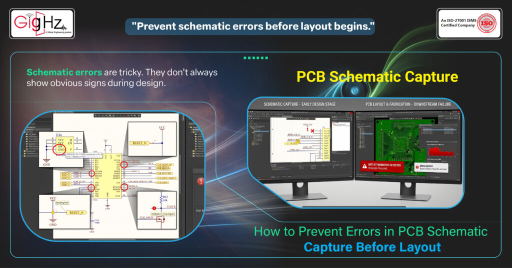
Ever had a PCB design that looked perfect in layout—but failed when it mattered most?
In many cases, the real problem isn’t in the layout at all.
It starts much earlier, during PCB schematic capture, where small mistakes can quietly go unnoticed.
Schematic errors are tricky. They don’t always show obvious signs during design.
A small issue—like a missed net connection, incorrect pin assignment, or unclear signal label—can quietly pass through unnoticed.
But once you reach layout, fabrication, or testing, these hidden mistakes can turn into costly delays, redesigns, and frustrating debugging sessions.
What makes this challenging is that these errors often hide in plain sight until it’s too late.
The good news?
You can prevent most of them with the right approach.
By focusing on accuracy and validation during schematic capture, you can avoid downstream issues and move into PCB layout with confidence and control.
But why do these errors occur so frequently in the first place—and why is prevention so critical?
Let’s take a closer look.
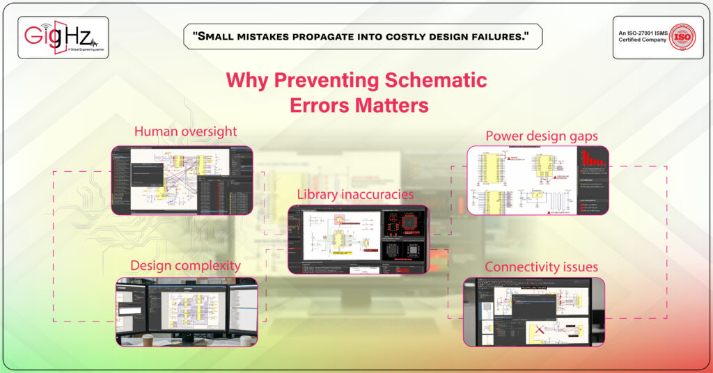
Why Preventing Schematic Errors Matters
A schematic is more than a drawing—it is the foundation of your PCB design. Every connection, component, and signal defined here directly impacts the final board.
When an error enters the schematic, it doesn’t stay there. It carries into layout, manufacturing, and testing, often leading to redesigns, rework, or even a full board respins.
Most errors come from common causes:
- Human oversight: Rushing or skipping checks
• Design complexity: Large or multi-sheet schematics
• Library inaccuracies: Incorrect symbols or footprints
• Power design gaps: Missing decoupling or poor grounding
• Connectivity issues: Floating nodes or incomplete nets
These small issues can lead to major problems, such as:
- Boards that fail to power up
• Noisy or unstable signals
• Circuit failures
• Assembly confusion
• Increased cost and delays
That’s why prevention matters. Fixing issues early is far easier than correcting them later.
Spending time validating your schematic reduces rework, improves workflow, and ensures a more reliable design.
A clean, verified schematic sets the path for a successful PCB.
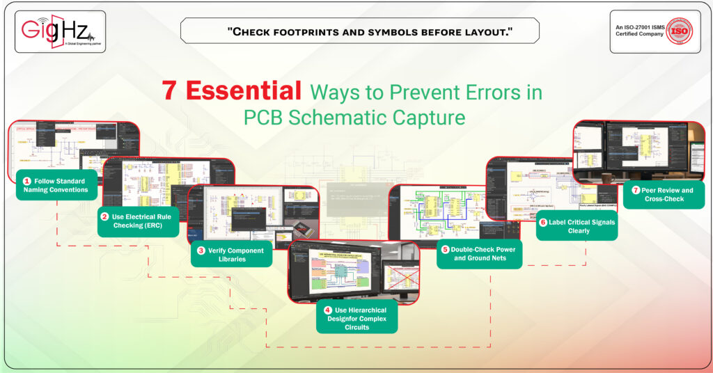
7 Essential Ways to Prevent Errors in PCB Schematic Capture
1. Follow Standard Naming Conventions
What happens:
Unclear or inconsistent naming conventions lead to confusion, incorrect connections, and misinterpretation during PCB design and layout.
How to prevent it:
• Use clear, descriptive net names like VCC_3V3, CLK_IN, RESET_OUT
• Avoid generic labels such as Net1 or unclear abbreviations
• Maintain consistent signal naming across all schematic sheets
• Define and follow a standard naming convention for the project
Quick Tip:
If a signal name is not instantly understandable, refine it before moving forward.
2. Use Electrical Rule Checking (ERC)
What happens:
Unconnected pins, voltage conflicts, or incorrect power nets go unnoticed and lead to functional failures later.
How to prevent it:
• Run Electrical Rule Checking (ERC) frequently during schematic capture
• Fix errors and warnings immediately
• Validate power connections and signal rules carefully
• Avoid postponing checks until the final stage
Quick Tip:
ERC is your first checkpoint—run it often and fix issues before they reach layout.
3. Verify Component Libraries
What happens:
Incorrect component libraries, symbols, or mismatched footprints result in assembly issues and non-functional boards.
How to prevent it:
• Cross-check symbols and footprints with manufacturer datasheets
• Validate pin mapping, package type, and electrical parameters
• Use verified or approved EDA libraries
• Maintain a centralized and version-controlled library system
Quick Tip:
Always double-check critical components—don’t rely blindly on library data.
4. Use Hierarchical Design for Complex Circuits
What happens:
Large, flat schematic designs become cluttered, increasing the risk of missing or incorrect connections.
How to prevent it:
• Break the design into smaller functional blocks
• Use hierarchical design for better organization
• Clearly define connections between blocks
• Review each block independently before integration
Quick Tip:
If your schematic looks crowded, restructure it into hierarchy for better clarity.
5. Double-Check Power and Ground Nets
What happens:
Improper power nets or floating ground connections cause instability, noise, or complete circuit failure.
How to prevent it:
• Ensure all ICs have proper power and ground connections
• Add decoupling capacitors near power pins
• Use consistent power net naming across the design
• Define a clear grounding strategy (analog vs digital if needed)
Quick Tip:
Every power pin should have a clear, verified connection—no exceptions.
6. Label Critical Signals Clearly
What happens:
Unlabeled or unclear critical signals lead to misrouting, noise issues, and performance problems during layout.
How to prevent it:
• Clearly label high-speed signals, analog signals, and sensitive nets
• Use consistent naming for signal groups and buses
• Highlight critical nets for easier review and routing
• Prepare signals for signal integrity (SI) and power integrity (PI) analysis
Quick Tip:
Label critical signals early to avoid routing errors and performance issues later.
7. Peer Review and Cross-Check
What happens:
Designers may overlook their own mistakes, especially in complex schematic designs.
How to prevent it:
• Conduct structured peer reviews before layout
• Use checklist-based validation for consistency
• Review schematics at multiple design stages
• Maintain version control and document design changes
Quick Tip:
A quick peer review can catch issues that hours of solo work might miss.
By following all these steps consistently, you ensure that your schematic is solid before moving to PCB layout.
Final Thoughts
Preventing errors in PCB schematic capture is not about adding complexity—it’s about following a consistent and disciplined process.
Each step, from verifying connections to reviewing designs, plays a key role in ensuring accuracy.
By focusing on connectivity, correct component usage, clear labeling, stable power design, simulation, and structured reviews, you can eliminate most errors before layout even begins.
The result is a smoother workflow, fewer design iterations, and a more reliable final product.
Small checks done early can prevent major issues later. Consistency matters. Attention to detail matters even more.
In the end, a well-prepared schematic is not just a starting point—it is the foundation of a successful PCB design.
Facing issues in PCB design?
Reach out to us — https://gighz.net/contact-us
If you need,
Book a Call. Schedule a Free Consultation now.
https://calendly.com/gighz/30min
Stuck in a loop of challenges? Always pick smart solution that works
Have you faced costly rework because 2D drawings skipped in MCAD workflows?
Effective way to prevent MCAD documentation errors recalls?
Please answer both poll questions before submitting.
Thank you for your response! 😊
Latest Post
Get Customized Engineering CAD Design Service

Book a Free Consultation Call
Partner with Gighz and bring your most innovative design concepts to life. Our engineering cad services accelerate development so you can focus on your big vision.
