

How to Route Traces Effectively in High-Density Interconnect PCB Boards
- Posted On:
- August 27, 2026
- Category:
- Ecad

High-Density Interconnect PCB are the backbone of today’s compact, high-performance electronics.
From smartphones and wearable devices to advanced IoT and medical gadgets, HDI boards allow engineers to pack more functionality into smaller spaces.
While this miniaturization offers incredible advantages, it also brings significant challenges. Routing traces, preserving signal integrity, and managing heat in dense, multilayer boards can quickly become complex—especially for high-speed circuits.
In this guide, we break down step-by-step strategies to route traces effectively in HDI PCBs, helping you optimize for performance, reliability, and manufacturability.
Whether you’re a designer or new to high-density layouts, these techniques will ensure your boards perform flawlessly.
Why Trace Routing in High-Density Interconnect PCB Matters
Routing traces in HDI PCBs is far more than simply connecting pins. Improper trace routing can lead to serious issues including signal degradation, crosstalk, electromagnetic interference (EMI), and thermal stress.
Each of these can compromise the reliability of the board, potentially leading to costly redesigns or product failures.
Effective trace routing ensures:
- Clean and stable signal paths
- Reduced electrical noise and interference
- Better thermal management
- Smooth manufacturing and assembly processes
Understanding the impact of trace routing at the design stage is critical.
A well-planned board not only performs better but also saves time and cost in production. The first step in effective routing is careful planning of the layer stack-up.
Step-by-Step Guide: Effective Trace Routing
Step 1: Plan the Layer Stack-Up
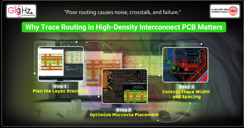
The layer stack-up forms the backbone of your High-Density Interconnect PCB, determining signal paths, impedance control, and thermal distribution.
Careful planning helps prevent congestion and interference.
- Mix signal, power, and ground layers strategically
- Include controlled impedance layers for high-speed signals
- Use thin dielectric layers to reduce board thickness
Collaborating with your manufacturer ensures your stack-up meets both electrical and thermal requirements.
Once your layers are defined, microvias can be placed to efficiently connect signals between layers.
Step 2: Optimize Microvia Placement
Microvias are tiny holes connecting layers, essential for saving space and maintaining performance. Proper microvia usage ensures reliable connections and minimizes manufacturing risks.
- Limit microvias to a single-layer depth
- Avoid stacking too many microvias
- Fill microvias when possible, to improve soldering strength
Thoughtful microvia placement prevents signal disruptions and maintains board integrity.
With microvias optimized, controlling trace width and spacing becomes crucial to prevent interference and maintain signal integrity.
Step 3: Control Trace Width and Spacing
Tight spacing in HDI designs makes trace width and spacing critical. Proper control prevents short circuits, crosstalk, and overheating.
- Ensure trace widths handle the required current
- Maintain spacing wide enough to avoid crosstalk
- Route high-speed differential pairs consistently
- Avoid sharp angles that disrupt signal flow
Correct trace dimensions prepare your board for smoother layer management and reduce potential routing conflicts.
Step 4: Manage Layers Efficiently

Altium automatically applies and checks:
- Clearance rules
- Routing constraints
- Width and via rules
This ensures that after conversion, your design is still manufacturing-ready.
5. Signal Integrity Awareness
For high-speed designs, conversion must preserve signal paths.
Altium supports:
- Basic signal integrity checks
- Controlled routing validation
This helps maintain integrity of critical nets like differential pairs.
6. Unified Environment
Everything—schematic, PCB, libraries, and outputs—is handled in one platform.
That means:
- No switching tools
- No data mismatch between modules
- Faster validation after conversion
In short, Altium focuses on preserving design intelligence while reducing manual effort during conversion.
How Zuken Handles EDA Conversion
Zuken is built for structured, high-complexity PCB workflows, commonly used in enterprise and system-level design environments.
Its modular architecture handles schematic, layout, and verification separately, which gives strong process control but adds coordination during conversion.
1. Separate Modules
Schematic, layout, and other features may work as separate modules.
During conversion, this can lead to:
- Extra steps to sync data
- More manual validation
This increases coordination effort during conversion.
2. Limited Built-in Simulation & Analysis
Compared to Altium, Zuken has fewer built-in tools for:
- Signal integrity
- Advanced simulation
- Field solving
So, engineers may need external tools to verify designs after conversion.
3. Component Mapping Complexity
Component libraries are not as tightly integrated.
This can result in:
- More manual footprint matching
- Increased risk of mismatched components
This adds additional effort during component alignment.
4. Workflow Overhead
Because of its structure, users may need to:
- Export/import between modules
- Perform separate checks
This increases overall conversion time.
In short, Zuken can handle conversion, but it often requires more manual work to ensure accuracy.
How to Choose the Right PCB Design Approach
From a practical perspective, choosing between Zuken vs Altium depends on project requirements and workflow structure rather than a fixed preference.
Different projects prioritize different factors:
- Some focus on strict process control and structured workflows
- Others focus on integrated environments and faster iteration
- Some require heavy validation stages, while others prioritize speed
The choice is generally influenced by:
- Project size and complexity
- Workflow structure
- Team collaboration model
- Conversion accuracy needs
- Validation requirements
In real engineering scenarios, both approaches are valid—the key is alignment with the project environment.
Final Thoughts
In a Zuken vs Altium comparison, EDA conversion is not just a small step—it directly affects your time, cost, and product quality.
Even small mistakes can lead to rework, delays, and added effort.
That’s why choosing the right platform matters. It’s not just about opening files, but keeping your design accurate and ready for manufacturing.
While Zuken offers flexibility, it often requires more manual work after conversion. This can slow things down, especially in complex projects.
On the other hand, Altium Designer makes the process smoother. With its unified environment and built-in validation, you can move to production faster with fewer errors.
If your goal is to save time and reduce errors, choosing the right tool can significantly improve overall design efficiency.
Book a Call. Schedule a Free Consultation now. https://calendly.com/gighz/30min
Stuck in a loop of challenges? Always pick smart solution that works
Have you faced costly rework because 2D drawings skipped in MCAD workflows?
Effective way to prevent MCAD documentation errors recalls?
Please answer both poll questions before submitting.
Thank you for your response! 😊
Latest Post
Get Customized Engineering CAD Design Service

Book a Free Consultation Call
Partner with Gighz and bring your most innovative design concepts to life. Our engineering cad services accelerate development so you can focus on your big vision.
