

Allegro to Altium: How to Import PCB Designs Without Errors
- Posted On:
- August 12, 2026
- Category:
- Ecad
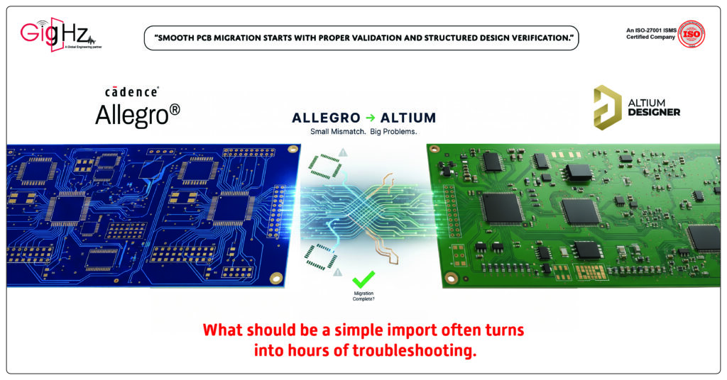
Switching PCB design tools might seem straightforward—but in reality, it rarely is.
When moving a design from Allegro to Altium, even a small mismatch can lead to missing footprints, broken nets, or incorrect layer mapping.
What should be a simple import often turns into hours of troubleshooting.
That’s because this process isn’t just about moving files—it’s about translating design data between two fundamentally different systems.
Without the right approach, important details can easily get lost in that translation.
The good news? These issues are completely avoidable.
With a structured method and proper validation, you can ensure a smooth and error-free transition.
Why Errors Happen During Allegro to Altium Import
Before jumping into the process, it helps to understand where things go wrong.
Allegro and Altium are built differently:
- Different data structures
- Different layer handling
- Different library systems
Because of this:
- Components may not map correctly
- Layers may shift or flip
- Nets can break silently
Key takeaway:
Errors don’t happen randomly—they happen when data is not properly prepared or verified.
What Data Must Be Preserved During Conversion
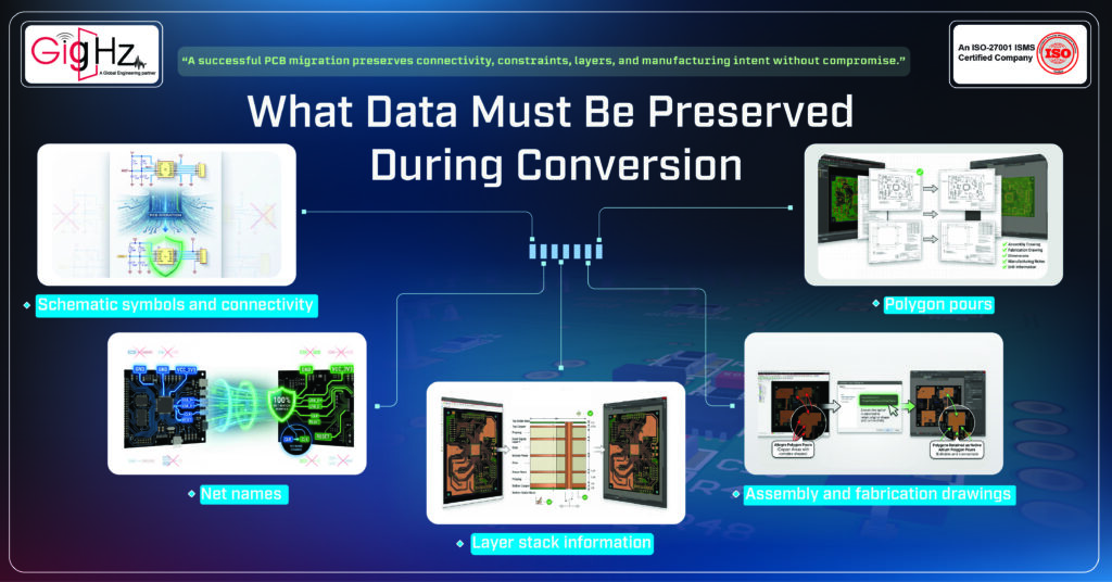
A successful migration involves much more than transferring copper geometry.
The converted project should retain:
- Schematic symbols and connectivity
- PCB footprints and pad definitions
- Net names
- Layer stack information
- Design rules
- Differential pair assignments
- Constraint settings
- Polygon pours
- Component parameters
- Manufacturing outputs
- Assembly and fabrication drawings
If any of this information is lost or altered, the translated design may no longer behave or manufacture as intended.
Common Import Errors During Allegro-to-Altium Conversion
One of the biggest misconceptions about EDA conversion is that the import process is fully automatic.
While Altium includes tools for importing Allegro databases, certain elements often require review and adjustment.
Typical issues include:
Footprints with incorrect pad shapes, missing net assignments, broken copper pours, altered layer mappings, lost constraints, and differential pairs that are no longer defined correctly.
Library references may also become disconnected, making future maintenance difficult.
Without proper validation, these errors can remain hidden until fabrication or testing.
Preparing the Allegro Design Before Export
The quality of the imported project depends heavily on the condition of the source database.
Before conversion, the Allegro design should be cleaned and verified.
Remove obsolete objects, confirm that the design passes rule checks, and ensure that layer names and stack definitions are clearly documented.
Exporting a known-good database reduces translation issues significantly.
Importing the Design into Altium
Altium provides import capabilities for Cadence design files.
During the import process, the software translates the schematic and layout data into native Altium project files.
Although the automated conversion saves time, it should be treated as the starting point rather than the final result.
Every critical design element must be reviewed to confirm that the translated project matches the source.
Validating the Converted Design
The most important part of the migration is validation.
The converted board should be compared against the original in terms of:
- Component placement
- Net connectivity
- Layer stack
- Trace widths and clearances
- Differential pair routing
- Plane and polygon behavior
- Design rules
- Drill data
- Gerber outputs
- Assembly documentation
A visual inspection alone is not sufficient.
The goal is to confirm that the new Altium project will produce the same manufacturing data and electrical behavior as the Allegro design.
Libraries and Long-Term Maintainability
Imported designs often contain temporary or unmanaged library data.
For long-term use, footprints and symbols should be organized into a structured library system within Altium.
This ensures that future revisions, ECOs, and component updates can be handled efficiently
Manufacturing Verification
Once the conversion is complete, generate fabrication outputs from Altium and compare them to the original release package.
This includes:
- Gerber files
- NC drill data
- Pick-and-place files
- Bill of materials
- Assembly drawings
Matching outputs provide confidence that the translation has preserved manufacturing intent.
Common Mistakes to Avoid
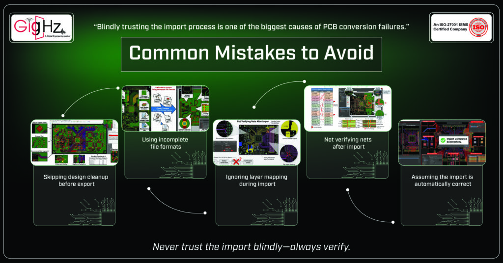
Here are the most common causes of errors during import:
- Skipping design cleanup before export
- Using incomplete file formats
- Ignoring layer mapping during import
- Not verifying nets after import
- Assuming the import is automatically correct
Never trust the import blindly—always verify.
Pro Tips for Error-Free Import
- Always use ODB++ or IPC-2581
- Validate your design before and after import
- Keep naming conventions simple
- Check connectivity early—not at the end
- Break the process into steps instead of rushing
Final Thoughts
Importing a PCB design from Allegro to Altium without errors is not about finding a perfect tool—it’s about following a disciplined process.
It comes down to three things:
- Preparation before export
- Accuracy during import
- Validation after import
When you control these three stages, most errors never happen in the first place.
A structured approach doesn’t just save time—it prevents costly mistakes and ensures your design moves forward without surprises.
“Avoid hours of debugging—get your PCB conversion right from the start.”
Book a Call. Schedule a Free Consultation now. https://calendly.com/gighz/30min
Stuck in a loop of challenges? Always pick smart solution that works
Have you faced costly rework because 2D drawings skipped in MCAD workflows?
Effective way to prevent MCAD documentation errors recalls?
Please answer both poll questions before submitting.
Thank you for your response! 😊
Latest Post
Get Customized Engineering CAD Design Service

Book a Free Consultation Call
Partner with Gighz and bring your most innovative design concepts to life. Our engineering cad services accelerate development so you can focus on your big vision.
