

How to Speed Up Time-to-Market with an Efficient PCB Design Process
- Posted On:
- August 7, 2026
- Category:
- Ecad

Getting a new electronic product to market quickly isn’t just a nice-to-have—it’s absolutely essential.
You have a great idea, a clear concept, maybe even a working prototype in mind.
But as soon as development starts, things can quickly go sideways.
A critical component might suddenly be unavailable, your layout could hit an unexpected snag, or the prototype simply doesn’t perform as expected.
Before you know it, your timeline has already slipped.
Most people blame complexity for delays. The truth? It’s often the PCB design process itself that isn’t fully prepared for real-world challenges.
Today’s electronics need to be smaller, faster, and more reliable, while development cycles continue to shrink and competition heats up.
Teams are expected to deliver high-quality products on time and within budget—that’s a lot of pressure to handle.
The solution: a well-structured process built to prevent delays before they even happen.
Why Design Development Gets Delayed
Let’s be honest—delays in design happen more often than you’d like.
And it’s rarely just one thing. Usually, it’s a combination of small hiccups along the way.
Some of the most common reasons include:
- Requirements that are unclear or keep changing
- Poor component selection without checking availability
- Design errors are identified during testing and later stages of development.
- Inefficient PCB layout design leading to routing challenges
- Poor coordination between design validation and manufacturing
These may seem minor initially, but in design, they quickly create a chain reaction of delays.
Step-by-Step: Build a Faster PCB Workflow
1. Start with Clear Design Requirements
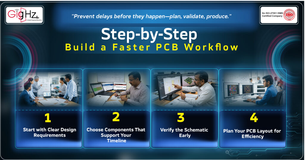
Clarity is everything.
Before diving into components or schematics,
Ask yourself:
What exactly does this product need to do, and how should it perform?
- Define functionality and performance expectations
- Avoid frequent changes once development begins
- Align with real-world applications and constraints
Doing this upfront reduces confusion and prevents costly rework later.
Once your requirements are solid, it’s time to choose components that support your timeline.
2.Choose Components That Support Your Timeline
Component selection isn’t just technical—it’s strategic.
- Pick widely available, reliable parts
- Avoid obsolete or high-risk components
- Keep backup options ready
Pro tip: Selecting multi-source components can prevent supply delays during production.
With components in place, the next step is to verify your schematic early.
3.Verify the Schematic Early
Your schematic is the backbone of your PCB design. Don’t wait until the end to check it.
- Review all connections carefully
- Validate power distribution
- Check critical signal paths and interfaces
Catching mistakes now saves big headaches later when you start layout and testing.
With your schematic solid, you can move on to planning the PCB layout efficiently.
4.Plan Your PCB Layout for Efficiency
A smart layout keeps your signals clean and your project moving.
- Optimize component placement based on function
- Simplify routing wherever possible
- Maintain clean and short signal paths
- Define proper trace width based on current and signal requirements
- Place vias strategically to minimize resistance, inductance, and signal loss
This step improves signal integrity and avoids redesign cycles, which is crucial for faster time-to-market.
Once your layout plan is ready, it’s time to run design checks continuously.
5.Run Design Checks Throughout the Process
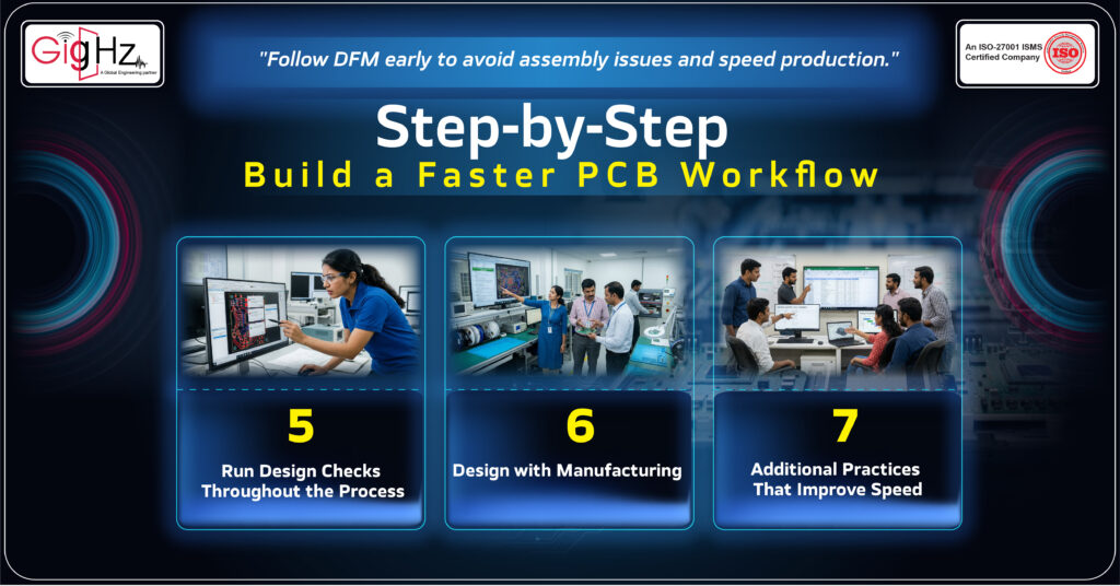
Validation isn’t something you do at the last minute.
- Perform design rule checks (DRC) regularly
- Fix spacing and routing issues early
- Validate design decisions at each stage
This keeps your design robust and reduces rework, ensuring your workflow never stalls.
Next, it’s important to design with manufacturing in mind.
6.Design with Manufacturing
Your design must be production-ready from the start.
- Follow design for manufacturability (DFM) guidelines
- Avoid overly complex stackups and structures
- Ensure easy assembly
Minimizing manufacturing issues early lets products move to market faster, without last-minute headaches.
Once your design is production-ready, you can further streamline the process with a few supporting practices that keep your workflow efficient.
7.Additional Practices That Improve Speed
Beyond the core steps, a few additional practices can further improve your process:
- Maintain proper documentation (BOM) at each stage
- Use version control for design files
- Improve communication between teams
- Use modern design tools for faster validation
These small but impactful practices keep everyone aligned and reduce confusion later on.
How This Improves Time-to-Market
When your PCB design process is efficient, the benefits are clear:
- Fewer redesign cycles
- Faster prototyping
- Reduced production issues
- Better coordination across teams
Instead of moving back and forth between stages, the process becomes smooth and predictable. Teams can focus on innovation rather than fixing repeated issues.
Final Thoughts
Speed in electronics development doesn’t come from rushing. It comes from building a process that prevents delays.
An efficient PCB design process helps you move from concept to production with fewer obstacles, better planning, and greater confidence.
By focusing on design optimization, validation, and manufacturability, you can significantly reduce development time while maintaining quality.
If your project is taking longer than expected, the issue may not be the design—it’s often the process behind it.
A strong PCB design workflow doesn’t just save time—it builds better, more reliable products.
In today’s fast-moving electronics industry, speed is not just an advantage—it’s a competitive necessity.
Book a Call. Schedule a Free Consultation now. https://calendly.com/gighz/30min
Stuck in a loop of challenges? Always pick smart solution that works
Have you faced costly rework because 2D drawings skipped in MCAD workflows?
Effective way to prevent MCAD documentation errors recalls?
Please answer both poll questions before submitting.
Thank you for your response! 😊
Latest Post
Get Customized Engineering CAD Design Service

Book a Free Consultation Call
Partner with Gighz and bring your most innovative design concepts to life. Our engineering cad services accelerate development so you can focus on your big vision.
