

How to Avoid Conversion Errors in OrCAD to Altium Conversion
- Posted On:
- August 19, 2026
- Category:
- Ecad
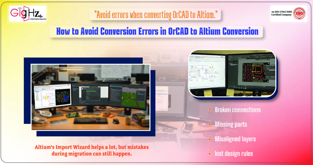
Moving your PCB designs from OrCAD to Altium Designer can be tricky, but it’s a common step for engineers who want better tools, faster design work, and smoother project management.
Altium’s Import Wizard helps a lot, but mistakes during migration can still happen.
These issues can cause broken connections, missing parts, misaligned layers, or lost design rules, which can slow down your project, create extra work, and even affect product quality.
In this guide, we will go through the top 10 most common errors that occur during migration and show simple, practical ways to avoid them.
Following these steps will help your designs stay correct, save valuable time, and make the process smoother, easier, and more reliable for your entire PCB workflow.
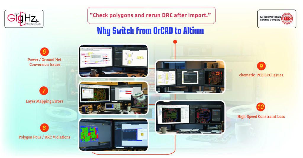
Why Switch from OrCAD to Altium
Before we dive into errors, it’s important to understand why engineers switch from OrCAD to Altium:
- Unified Design Environment: Altium integrates schematic capture and PCB layout in one tool, reducing mismatches and errors.
- Advanced Routing & High-Speed Support: Altium handles HDI and complex routing more efficiently than OrCAD.
- Company Standardization: Many teams migrate to a single EDA platform to streamline collaboration and licensing.
With these advantages, investing time to avoid conversion errors is well worth it.
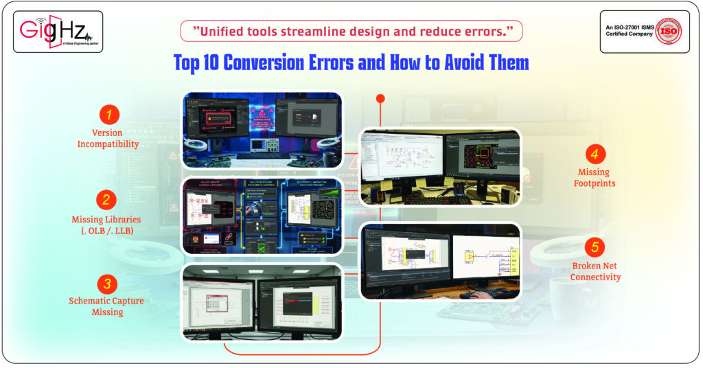
Top 10 Conversion Errors and How to Avoid Them
Here’s a structured flow of common conversion errors, in the order they typically occur, and how to handle them effectively:
1. Version Incompatibility
Problem: OrCAD files from newer versions may fail to import, showing messages like “Unrecognized Project File Version.”
Solution:
- Check your OrCAD version before import.
- Save files in a compatible format if your Altium Designer version doesn’t support the current OrCAD release.
Tip: Altium Designer Summer 09 or later works well for OrCAD 10.x and above.
2. Missing Libraries (. OLB /. LLB)
Problem: Schematic symbols (.OLB) or PCB footprints (.LLB) may not be found during import.
Solution:
- Gather all library files locally or ensure network access.
- Include these files in the Import Wizard session.
- Verify that all library links are correctly mapped post-import.
3. Schematic Capture Missing
Problem: Imported schematics may be incomplete or missing entirely.
Solution:
- Ensure the. DSN schematic files are included.
- Run Design Rules Check (DRC) in OrCAD to catch hidden issues before import.
- Validate that hierarchical or off-page connectors are mapped correctly in Altium.
4. Missing Footprints
Problem: Components appear in schematics but lack associated PCB footprints.
Solution:
- Import both. OLB and .LLB files.
- Check that footprint references in the schematic are correct.
- Verify each component visually in the PCB editor
5. Broken Net Connectivity
Problem: Some nets may appear disconnected, causing design errors.
Solution:
- Compile the project in Altium after import to identify unconnected pins or nets.
- Ensure off-page connectors are correctly converted to Altium ports.
- Manually reconnect any missed nets, especially in complex multi-sheet designs.
6. Power / Ground Net Conversion Issues
Problem: Power and ground nets may not translate correctly from OrCAD to Altium.
Solution:
- Altium uses Power Ports instead of global nets.
- Verify all VCC, GND, and other power nets are connected correctly.
- Check for missing connections in hierarchical or multi-page designs.
7. Layer Mapping Errors
Problem: OrCAD and Altium have different layer naming conventions, leading to misplaced traces, overlays, or mechanical layers.
Solution:
- Map layers carefully during the Import Wizard step:
- Top → Top Layer
- Bottom → Bottom Layer
- SMT / SST → Top / Bottom Overlay
- Assembly → Mechanical Layers
- Save custom mappings as reusable .INI files for multiple projects.
8. Polygon Pour / DRC Violations
Problem: Copper pours may appear incomplete, and DRC violations may surface post-import.
Solution:
- Check polygons and repour them as needed.
- Run Design Rule Check to catch clearance or overlap issues.
- Adjust thermal relief and clearance settings if polygons are misaligned.
9. Schematic ↔ PCB ECO Issues
Problem: Engineering Change Orders (ECOs) may show unexpected changes, leading to inconsistencies between schematic and PCB.
Solution:
- Open both schematic and PCB projects in Altium.
- Run Design → Import Changes and carefully review the ECO dialog.
- Investigate any unexpected changes before accepting, focusing on component references and net names.
10. High-Speed Constraint Loss
Converting OrCAD to Altium Designer doesn’t have to be overwhelming.
Most errors—like missing libraries, broken net connectivity, or layer mapping issues—can be avoided with proper preparation and careful verification.
By focusing on the 10 key conversion errors, engineers can systematically address potential problems, reduce post-import fixes, and ensure both schematics and PCB layouts remain accurate.
The workflow is straightforward: prepare → import → verify → fix → validate.
Following this approach helps maintain design integrity, save time, and prevent costly mistakes.
A careful and methodical migration not only ensures error-free designs but also improves team collaboration, supports high-speed and complex PCB requirements, and fully leverages Altium Designer’s advanced capabilities for a smoother, more reliable PCB design process.
Final Thoughts
PCB design is complex, but HDI provides practical and effective solutions.
Dense components?
High-speed signals?
Tight spaces?
Challenging layouts?
HDI has the tools to solve them all. Microvias, advanced fanout strategies, and smart layer planning help reduce routing errors, improve signal and power integrity, and save valuable design time.
Applying HDI techniques leads to less rework, lower production costs, and more reliable, high-performance boards.
For engineers working on modern electronics—prototypes, high-speed circuits, or compact designs—HDI is the key to smarter, more efficient, and dependable PCB design.
Start planning your HDI layouts today and overcome PCB design challenges with confidence.
Book a Call. Schedule a Free Consultation now. https://calendly.com/gighz/30min
Stuck in a loop of challenges? Always pick smart solution that works
Have you faced costly rework because 2D drawings skipped in MCAD workflows?
Effective way to prevent MCAD documentation errors recalls?
Please answer both poll questions before submitting.
Thank you for your response! 😊
Latest Post
Get Customized Engineering CAD Design Service

Book a Free Consultation Call
Partner with Gighz and bring your most innovative design concepts to life. Our engineering cad services accelerate development so you can focus on your big vision.
