

How to Overcome PCB Design Challenges with Advanced HDI Solutions
- Posted On:
- August 14, 2026
- Category:
- Ecad
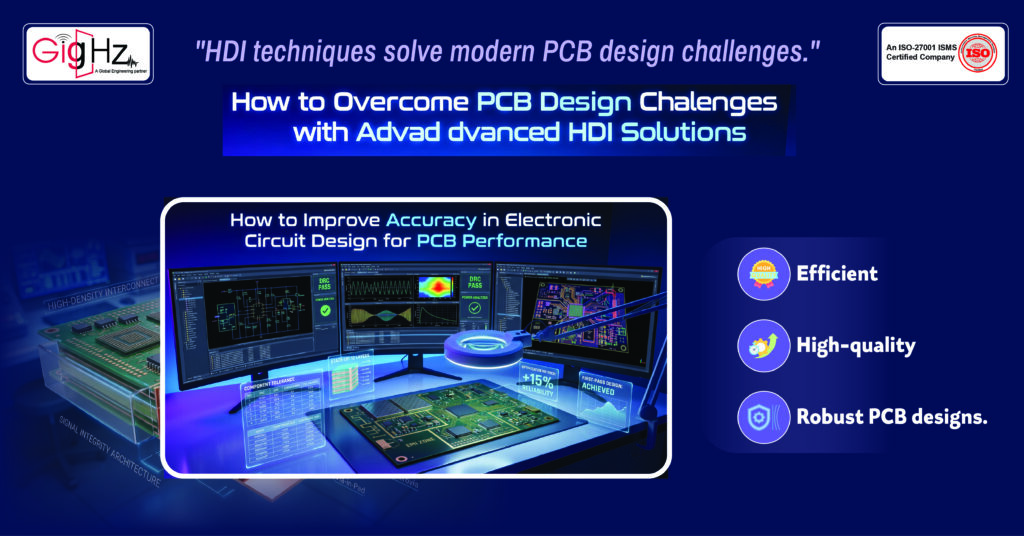
Modern electronics are evolving faster than ever.
Devices are becoming smaller, smarter, and packed with more features than ever before.
Tighter boards, complex routing, and high-speed signals create significant challenges for designers.
Crowded layouts, signal integrity issues, and thermal problems can lead to design delays, repeated prototypes, and higher costs.
Even a minor oversight in component placement or routing can ripple into major performance or reliability problems.
This is where High-Density Interconnect (HDI) techniques prove invaluable. By using microvias, optimized layer layouts, and advanced fanout strategies, engineers can create compact, reliable, high-performance boards that meet the demands of modern electronics.
With smart HDI planning, designers can handle dense and fine-pitch components efficiently, reduce production errors, minimize costly redesigns, and deliver faster time-to-market.
In this guide, we’ll explore the key PCB design challenges and demonstrate practical HDI solutions that help engineers achieve efficient, high-quality, and robust PCB designs.
Common PCB Design Challenges
Understanding the hurdles is the first step toward solving them.
Let’s look at the main challenges modern PCB designers face:
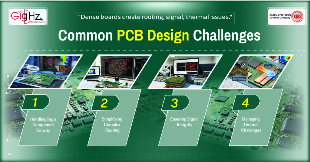
- High Component Density – With more features packed into smaller devices, boards are getting crowded. This makes routing tricky and increases the risk of assembly errors.
- Complex Routing – Multi-layer boards often lead to congested traces and overlapping signals. Without careful planning, this can affect performance and reliability.
- Signal Integrity Issues – High-speed signals are vulnerable to noise, crosstalk, and reflections, which can degrade performance or cause functional failures.
- Thermal Management – Dense boards generate heat. Inadequate thermal design can damage components and reduce board lifespan.
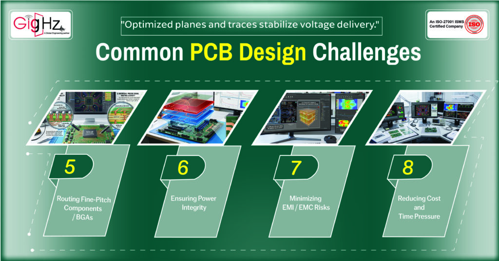
- Fine-Pitch Components / BGAs – Ultra-fine pitches (for example, 0.37 mm) are challenging to route, increasing the risk of shorts, lost signals, or manufacturing issues.
- Power Integrity – Voltage drops or unstable power rails can disrupt circuit operation, especially in high-speed designs.
- EMI / EMC – Radiated interference can lead to regulatory compliance failures and unpredictable circuit behavior.
- Cost and Time Pressures – Tight budgets and deadlines make repeated prototyping expensive and stressful.
HDI Solutions for Key PCB Challenges
Now let’s see how HDI techniques help designers tackle these problems.
Crowded layouts can cause routing errors, slow down production, and increase failure rates.
HDI Solutions:
- Microvias connect layers efficiently without taking up extra space.
- Smaller traces and pads allow components to sit closer together.
- Optimized HDI layouts balance density with accessibility for assembly and testing.
Tip for Designers: Plan component placement carefully. Group related parts together to keep routing simple and short.
Benefit: Compact, clean boards that are functional and reliable.
2. Simplifying Complex Routing
Multi-layer boards can get messy fast. Without proper planning, traces overlap, and interference can creep in.
HDI Solutions:
- Blind and buried vias connect only the layers you need, reducing congestion.
- Layer stack-up optimization gives critical signals dedicated paths.
Practical Insight: Simulate routing early. Spot bottlenecks before they become costly problems.
Benefit: Smooth routing, fewer errors, and better signal quality.
3. Ensuring Signal Integrity
Fast signals are sensitive—crosstalk, reflections, and noise can quickly create problems.
HDI Solutions:
- Controlled impedance routing keeps signals clean.
- Layer planning separates sensitive signals from noisy ones.
- SI/PI simulations catch issues before fabrication.
Tip for Designers: Always validate high-speed paths with simulations. Use guard traces where needed.
Benefit: Stable signals and reliable high-speed performance.
4. Managing Thermal Challenges
Excess heat silently damages components, affecting performance and lifespan.
Thermal management is a frequent PCB design challenge in dense boards.
HDI Solutions:
- Use heat-resistant materials for critical layers.
- Arrange layers to distribute heat efficiently.
- Run thermal simulations to detect hotspots early.
Practical Tip: Include thermal vias under high-power components to improve heat dissipation.
Benefit: Longer component life and higher board reliability.
5. Routing Fine-Pitch Components / BGAs
Ultra-fine-pitch BGAs need precise routing to avoid shorts or lost signals.
HDI Solutions:
- Via-in-pad ensures reliable connectivity without enlarging the board footprint.
- Microvias maintain strong connections even in dense layouts.
Designer Tip: Always check manufacturing tolerances for fine-pitch components.
Benefit: Reliable connections in compact, high-performance boards.
6. Ensuring Power Integrity
Stable power is crucial for performance.
HDI Solutions:
- Design a robust power distribution network (PDN) for stable voltage delivery
• Use dedicated power and ground planes for low impedance paths
• Optimize trace width and via structures for current handling
• Add decoupling capacitors close to IC power pins
• Run power integrity simulations before manufacturing
Benefit: Consistent voltage, reduced noise, and dependable operation.
7. Minimizing EMI / EMC Risks
Radiated interference can be a hidden problem.
HDI Solutions:
- Use shielding and optimized trace
- Plan stack-ups and grounding to minimize emissions.
- Run EMI/EMC simulations early to catch issues.
Benefit: Compliant, interference-free boards.
8. Reducing Cost and Time Pressure
Tight budgets and repeated prototypes create stress—a common PCB design challenge.
HDI Solutions:
- Apply DFx design practices to reduce errors.
- Optimize component selection and layout.
- Validate designs with early simulations.
Benefit: Faster, cost-efficient production of high-quality PCBs
Final Thoughts
PCB design is complex, but HDI provides practical and effective solutions.
Dense components?
High-speed signals?
Tight spaces?
Challenging layouts?
HDI has the tools to solve them all. Microvias, advanced fanout strategies, and smart layer planning help reduce routing errors, improve signal and power integrity, and save valuable design time.
Applying HDI techniques leads to less rework, lower production costs, and more reliable, high-performance boards.
For engineers working on modern electronics—prototypes, high-speed circuits, or compact designs—HDI is the key to smarter, more efficient, and dependable PCB design.
Start planning your HDI layouts today and overcome PCB design challenges with confidence.
Book a Call. Schedule a Free Consultation now. https://calendly.com/gighz/30min
Stuck in a loop of challenges? Always pick smart solution that works
Have you faced costly rework because 2D drawings skipped in MCAD workflows?
Effective way to prevent MCAD documentation errors recalls?
Please answer both poll questions before submitting.
Thank you for your response! 😊
Latest Post
Get Customized Engineering CAD Design Service

Book a Free Consultation Call
Partner with Gighz and bring your most innovative design concepts to life. Our engineering cad services accelerate development so you can focus on your big vision.
