

How to Apply Design for Manufacturability (DFM) in PCB Design
- Posted On:
- July 16, 2026
- Category:
- Ecad

Have you ever spent hours designing a PCB only to discover it can’t be manufactured efficiently?
Frustrating, right? You’re not alone.
Many hardware startups, engineers, and electronics designers hit the same wall—your brilliant idea looks perfect on screen, but real-world production tells a different story.
That’s where Design for Manufacturability (DFM) comes in.
Think of DFM as a bridge between engineering creativity and factory reality.
It’s more than a checklist—it’s a mindset.
Designing with manufacturing and assembly in mind from day one saves time, reduces errors, and ensures your PCB works as intended once it hits the production line.
DFM ensures your board is easy to build, cost-effective, and reliable. In this guide, we’ll cover practical steps—from component placement to panelization—to make your PCBs production-ready.
By the end, you’ll know how to design smarter, avoid common pitfalls, and bring your hardware product to market faster.
Why Design for Manufacturability (DFM) Matters in PCB Design
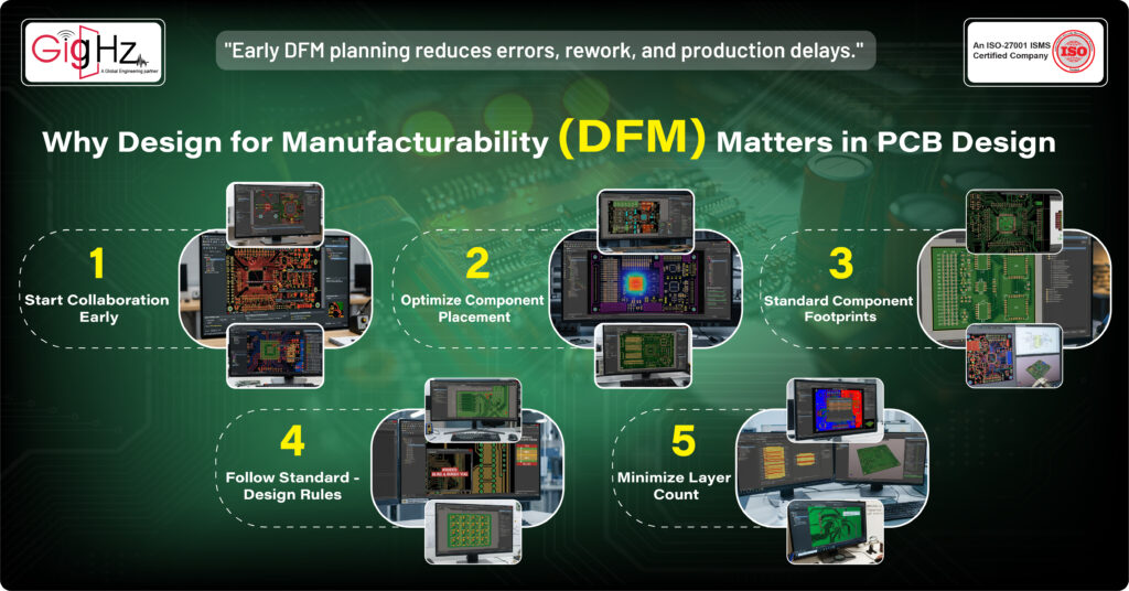
Before you start designing, understand why DFM is key:
- Know your manufacturer: Trace widths, drill sizes, and tolerances matter.
- Plan for assembly: Think pick-and-place, test points, and component orientation.
- Balance design and manufacturability: Materials and stackup affect performance and reliability.
- Avoid costly errors: Early DFM reduces rework, failures, and delays.
This quick prep ensures the steps that follow are faster, easier, and more reliable.
1. Start Collaboration Early
Don’t wait until the board is done. Talk to your manufacturer and assembly team from the beginning.
Benefits of early collaboration:
- Catch design rule violations before production
- Avoid incompatible materials or solder mask issues
- Fix component spacing and clearance problems
- Reduce costly rework and surprises
Early alignment keeps your PCB design in line with real-world capabilities. Regular feedback sessions also reveal hidden risks and help optimize materials and assembly processes.
2. Optimize Component Placement
Component placement affects signal integrity, thermal performance, and assembly efficiency.
Placement tips:
- Align similar components in the same orientation
- Keep large parts away from fine-pitch devices
- Leave room for test points, connectors, and inspection
- Ensure automated tools can access all areas
Smart placement reduces soldering defects, inspection failures, and assembly delays.
Consider automated pick-and-place accessibility for every component to save time and improve consistency.
3. Standard Component Footprints
“Standard footprints ensure compatibility, reduce errors, and simplify manufacturing.”
Use industry-standard packages and follow datasheet-recommended land patterns.
Best practices:
- Use common package sizes (0603, SOIC, QFN)
- Verify with datasheets
- Maintain proper pad spacing
- Avoid custom footprints
Standard footprints improve soldering quality, reduce defects, and ensure smooth automated assembly.
4. Follow Standard Design Rules
Consistent design rules simplify manufacturing. Avoid unnecessary complexity wherever possible.
Key DFM practices:
- Use standard trace widths, via sizes, and pad spacing
- Avoid blind or buried vias unless necessary
- Stick to standard panel sizes
- Maintain consistent solder mask clearances
Standardization reduces layer count issues, speeds assembly, and improves yield. It also simplifies quality checks.
5. Minimize Layer Count
Extra layers increase complexity, drilling time, and costs.
DFM tips:
- Consolidate signal layers when feasible
- Optimize power and ground planes
- Keep vias and routing efficient
Simpler stacks improve consistency, especially for low-volume or high-mix boards. Fewer layers also mean reduced drilling errors and faster turnaround.
6. Apply Trace Routing for Reliability
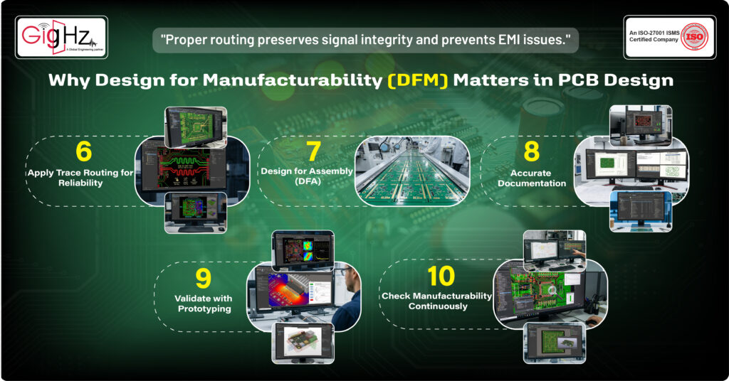
Signal integrity is critical, especially for high-speed circuits. Proper routing prevents EMI and reduces test failures.
Routing rules:
- Keep high-speed traces short and straight
- Avoid 90° angles; use 45° bends
- Match lengths for differential pairs
- Maintain continuous return paths
Following these steps reduces field failures and improves assembly yields. It also ensures signal integrity across analog and digital circuits.
7. Design for Assembly (DFA)
Design for Manufacturability (DFM) isn’t complete without considering assembly. Your board must be machine-friendly.
DFA best practices:
- Include reference markers for automated vision
- Optimize panelization for conveyor systems
- Provide accessible test points
- Clearly mark component polarity
Designing for assembly ensures faster production, fewer errors, and easier PCB fabrication and testing.
8. Accurate Documentation
Even perfect boards fail without clear documentation.
Include:
- Fabrication and assembly drawings
- Updated Bill of Materials (BOM)
- Gerber files, pick-and-place data
- Test and inspection procedures
Documentation ensures engineers, manufacturers, and testers are on the same page. It also helps with regulatory compliance and long-term reliability.
9. Validate with Prototyping
Prototyping reveals real-world issues that design reviews can miss.
What to test:
- Component fit and orientation
- Connector accessibility
- Thermal performance (heat sinks, thermal vias)
- Signal integrity and EMI
A well-tested prototype prevents costly redesigns and ensures your PCB will perform reliably at scale.
10. Check Manufacturability Continuously
It’s not a one-time check. Review at every stage:
- Early schematic: check stackup and material choices
- Mid-layout: verify component spacing and trace routing
- Pre-production: validate panelization and assembly readiness
Continuous checks reduce first-pass failures and improve time-to-market.
How DFM Improves PCB Production
Applying DFM brings measurable benefits:
- Higher first-pass yield – fewer boards rejected
- Lower rework rate – reduce manual fixes
- Faster production – streamlined assembly
- Lower cost per board – fewer errors, less scrap
- Improved reliability – consistent thermal performance and signal integrity
DFM turns your PCB design into a product that’s reliable, repeatable, and ready for mass production. It also allows faster iteration cycles, helping startups launch products quicker with confidence.
Quick DFM Checklist for PCB Design
- Placement: Machine-friendly orientation
- Spacing: Adequate solder and assembly clearance
- Materials: Approved stackup for reliability
- Testing: Accessible test points
- Panelization: Optimized for assembly line
Following this checklist ensures your design is manufacturable and high-quality.
Final Thoughts
DFM is your roadmap to efficient PCB production. By applying these principles early:
- Align with manufacturers
- Optimize component placement and routing
- Choose the right materials
- Validate with prototyping and testing
You reduce errors, save costs, and deliver a reliable product. Every step from layout to assembly matters.
Start with Design for Manufacturability (DFM) in PCB design, and your boards will be easier to fabricate, assemble, and test.
Planning your next PCB project?
Let’s make it production-ready. https://gighz.net/contact-us
Book a Call. Schedule a Free Consultation now. https://calendly.com/gighz/30min
Stuck in a loop of challenges? Always pick smart solution that works
Have you faced costly rework because 2D drawings skipped in MCAD workflows?
Effective way to prevent MCAD documentation errors recalls?
Please answer both poll questions before submitting.
Thank you for your response! 😊
Latest Post
Get Customized Engineering CAD Design Service

Book a Free Consultation Call
Partner with Gighz and bring your most innovative design concepts to life. Our engineering cad services accelerate development so you can focus on your big vision.
