

KiCad to Altium Conversion: Step-by-Step PCB Migration Guide
- Posted On:
- July 10, 2026
- Category:
- Ecad

Moving a PCB from KiCad to Altium can seem tricky, especially when working with multi-layer boards. But it doesn’t have to be.
Whether it’s a small prototype or a complex multi-layer, high-speed board, having a clear and structured plan makes the process much easier.
Every detail counts — PCB layout, schematic verification, power distribution, and signal integrity.
Each step affects the final performance of your board.
Even small mistakes during EDA conversion can break nets, create voltage drops, or cause functional issues that are costly to fix later.
Following a structured workflow keeps your process smooth, reduces errors, and saves time.
This step-by-step guide walks you through PCB migration, providing practical tips, examples, and advice to make your board accurate, reliable, and production-ready from start to finish.
Why Migrate from KiCad to Altium?
KiCad is a fantastic open-source PCB tool, perfect for hobbyists and small projects. But when your designs grow in complexity, or you need advanced features like high-speed simulation, advanced layer management, and robust library handling, Altium Designer becomes a tempting upgrade.
Some key reasons engineers migrate:
- Advanced routing and design rule capabilities in Altium
- Better library management and 3D modeling
- Collaboration with large teams or clients who use Altium
- Access to simulation, signal integrity (SI), and power integrity (PI) tools
So, if you’ve made up your mind, let’s look at how to make the transition without headaches.
Step-by-Step KiCad to Altium Conversion
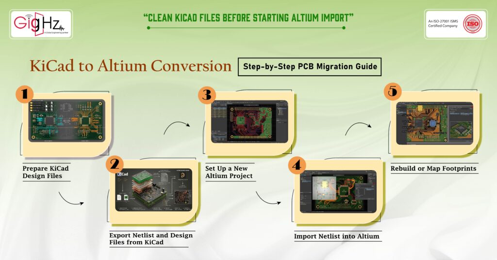
Step 1: Prepare KiCad Design Files
Before you even open Altium, clean up your KiCad files. A messy source can cause unnecessary headaches later.
Checklist for prep:
- Update all footprints and symbols – ensure libraries are up-to-date.
- Check schematic connectivity – no broken nets or undefined components.
- Clean up PCB layout – remove unused layers, nets, or vias.
- Back up your project – always keep a safe copy in case something breaks.
Think of this as tidying up before moving house—it makes unpacking in Altium much smoother.
Step 2: Export Netlist and Design Files from KiCad
Altium doesn’t natively open KiCad files, so we need an intermediate step. The most reliable way is exporting a netlist.
- Open your KiCad project.
- Go to Tools → Generate Netlist.
- Choose Spice or PCBNew Netlist format (Altium works well with Pcbnew XML/Netlist).
- Export Gerber files for reference—it’s handy for layer mapping.
Tip: Keep your netlist and Gerbers together in a single folder. It makes the import process easier and reduces mistakes.
Step 3: Set Up a New Altium Project
Now, open Altium Designer and set up a new project:
- Go to File → New → Project → PCB Project.
- Name it similarly to your KiCad project to avoid confusion.
- Configure project settings:
- Units (mm vs mils)
- Layers (signal, power, mechanical)
- Design rules (track width, via sizes, clearances)
Pro Tip: Align Altium’s layer stack with KiCad’s layers. This avoids misalignment issues during import
Step 4: Import Netlist into Altium
Here comes the magic:
- In Altium, go to Project → Import → Netlist.
- Select your KiCad-generated netlist.
- Map symbols and footprints manually if needed—Altium may not recognize custom KiCad symbols.
- Verify imported schematic connections in Altium’s schematic editor.
Friendly tip: Don’t skip this verification. Even a single missing net can ruin your PCB later.
Step 5: Rebuild or Map Footprints
KiCad and Altium use different libraries. You have two options:
- Manual footprint mapping – match KiCad footprints to Altium libraries.
- Create custom footprints – import 3D models or recreate footprints for components missing in Altium.
Tip: Altium’s 3D view is fantastic for checking footprints before routing. A quick visual check saves hours during manufacturing.
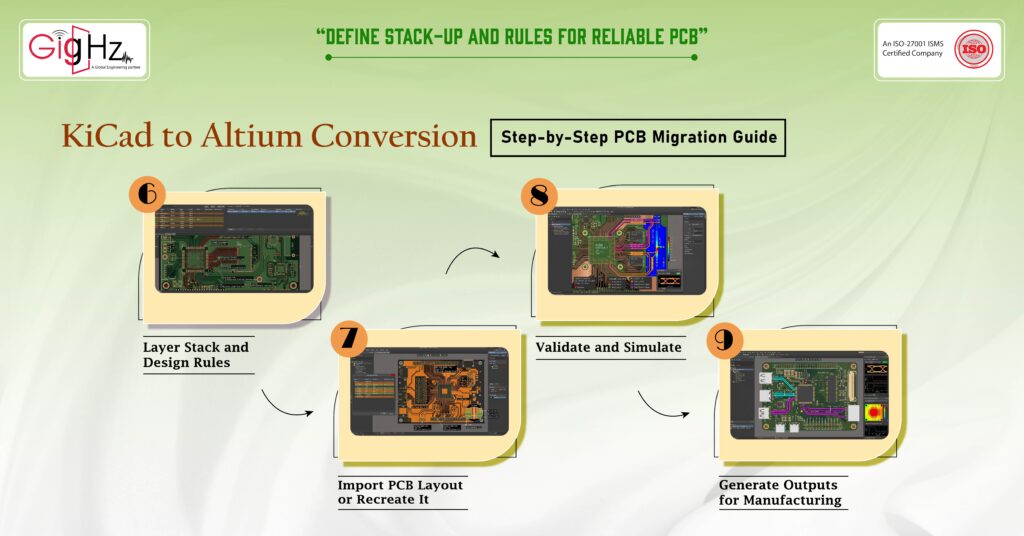
Step 6: Layer Stack and Design Rules
Next, configure your PCB stackup and design rules:
- Define signal and power layers based on your KiCad design.
- Set clearances, via types, and trace widths according to your project requirements.
- Add impedance constraints if your PCB is high-speed.
Altium offers powerful rule-based checks. Use them now to catch issues before routing.
Step 7: Import PCB Layout or Recreate It
Altium doesn’t directly import KiCad PCB layouts, so you have two approaches:
- Manual Recreation – overlay Gerbers as a reference and route traces in Altium.
- Use intermediate formats – some engineers export DXF or ODB++ from KiCad and import them into Altium for reference.
Pro Tip: Treat this like tracing a blueprint—you’re not copying, you’re translating
Step 8: Validate and Simulate
Once your schematic and layout are imported and footprints are mapped:
- Run Design Rule Check (DRC) in Altium.
- Simulate critical nets for signal integrity and power integrity.
- Double-check via types, net classes, and differential pairs.
This step ensures your migrated PCB is not just visually correct but electrically sound.
Step 9: Generate Outputs for Manufacturing
Finally, prepare your outputs:
- PCB fabrication files (Gerbers, ODB++, IPC-2581)
- Assembly drawings and pick-and-place files
- Bill of Materials (BOM)
- 3D render for mechanical verification
By now, your project is fully in Altium Designer, ready for production or prototyping
Bonus Tips for a Smooth Migration
- Start small – test the migration with one simple board before moving your flagship project.
- Keep KiCad files – in case you need to reference or troubleshoot anything later.
- Document changes – note any footprint changes or rule adjustments for future reference.
- Leverage Altium’s community – forums, webinars, and tutorials can save hours.
Final Thoughts
Migrating from KiCad to Altium may feel like a lot of work, but it’s manageable if you approach it methodically.
Clean up your KiCad project, export carefully, verify connections, map footprints, and use Altium’s advanced rules and simulation tools to validate your design.
Once done, you’ll enjoy Altium’s powerful features, better collaboration, and advanced PCB capabilities—all while keeping your original design intact.
Think of it as upgrading your design toolkit without losing your project’s soul.
Book a Call. Schedule a Free Consultation now. https://calendly.com/gighz/30min
Stuck in a loop of challenges? Always pick smart solution that works
Have you faced costly rework because 2D drawings skipped in MCAD workflows?
Effective way to prevent MCAD documentation errors recalls?
Please answer both poll questions before submitting.
Thank you for your response! 😊
Latest Post
Get Customized Engineering CAD Design Service


Book a Free Consultation Call
Partner with Gighz and bring your most innovative design concepts to life. Our engineering cad services accelerate development so you can focus on your big vision.
