

PCB Power Plane Design Best Practices Every Engineer Should Know
- Posted On:
- October 12, 2026
- Category:
- Ecad

Your PCB passes design rule checks (DRC), signal routing looks clean, and manufacturing is complete.
Yet during testing, the FPGA resets unexpectedly, DDR memory becomes unstable, or analog measurements fluctuate under heavy processing loads.
If the schematic is correct, where is the problem?
In many high-speed designs, the issue lies in the power plane. A poorly designed power distribution network (PDN) struggles to deliver clean, stable power when components demand rapid bursts of current. The result is voltage droop, power noise, ground bounce, electromagnetic interference (EMI), and reduced system reliability.
Optimizing PCB power plane design isn’t about adding more copper. It’s about creating a low-impedance path that delivers stable power under real operating conditions. Here’s how experienced PCB designers achieve it.
What Is PCB Power Plane Design?

A PCB power plane is a dedicated copper layer that distributes power with low resistance and inductance, improving current flow and thermal performance.
Together with a continuous ground plane, it supports stable power delivery for processors, FPGAs, memory, and high-speed interfaces.
Poor design can cause voltage drops, noise, uneven current distribution, and thermal stress, leading to power integrity and reliability problems.
Why Poor Power Plane Design Causes Problems
Modern ICs rarely draw constant current. Instead, they demand rapid bursts of current within nanoseconds. If the PDN cannot respond quickly, the supply voltage temporarily drops.
For example, a processor operating at 1.0 V with a maximum allowable ripple of 50 mV and a peak transient current of 2 A requires a PDN impedance of approximately 25 mΩ (0.05 V ÷ 2 A). Exceeding this value can cause timing errors, clock jitter, unexpected resets, and unstable communication.
Poor power plane design may also lead to:
- Voltage drops
- Simultaneous Switching Noise (SSN)
- Increased EMI
- Localized heating
- Reduced signal integrity
Good power integrity begins with controlling impedance rather than simply increasing copper area.
PCB Power Plane Design Best Practices
1. Design for Low PDN Impedance
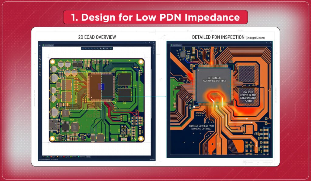
Power integrity is fundamentally an impedance problem. Wide, continuous copper planes provide multiple current paths that reduce both resistance and inductance.
Avoid narrow copper necks, isolated copper islands, and unnecessarily long current paths. Even a small bottleneck can restrict transient current flow, causing voltage drop during peak switching activity.
2. Keep Power and Ground Planes Adjacent
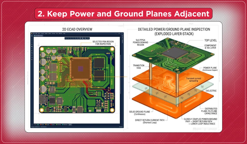
Place the power plane directly next to a solid ground plane whenever possible.
This reduces loop inductance, improves return current paths, and creates distributed plane capacitance that supports high-frequency current demands. A closely coupled power-ground pair also improves EMC performance and reduces power supply noise.
3. Optimize Decoupling Capacitor Placement

The effectiveness of a decoupling capacitor depends more on loop inductance than on capacitance value alone.
Position capacitors as close as possible to IC power pins with short connections to both power and ground planes. Designers often combine 10 µF, 1 µF, 100 nF, and 10 nF capacitors to maintain low impedance across different frequency ranges, ensuring stable voltage during rapid switching.
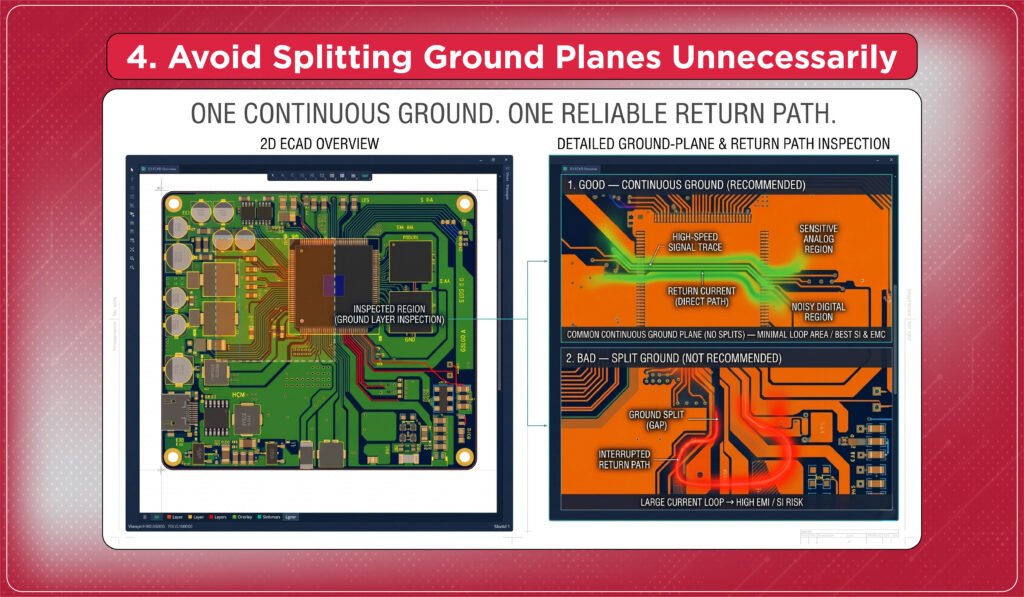
4. Avoid Splitting Ground Planes Unnecessarily
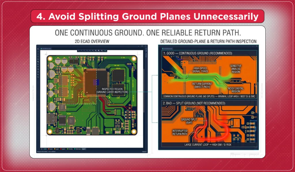
A common misconception is that separating analog and digital grounds always reduces noise.
For most modern high-speed PCBs, a continuous ground plane is the better choice. Splitting the plane interrupts return current paths, increases loop area, and may worsen EMI and signal integrity when high-speed traces cross the split.
Instead, isolate noisy and sensitive circuits through intelligent placement and routing while maintaining one uninterrupted ground reference.
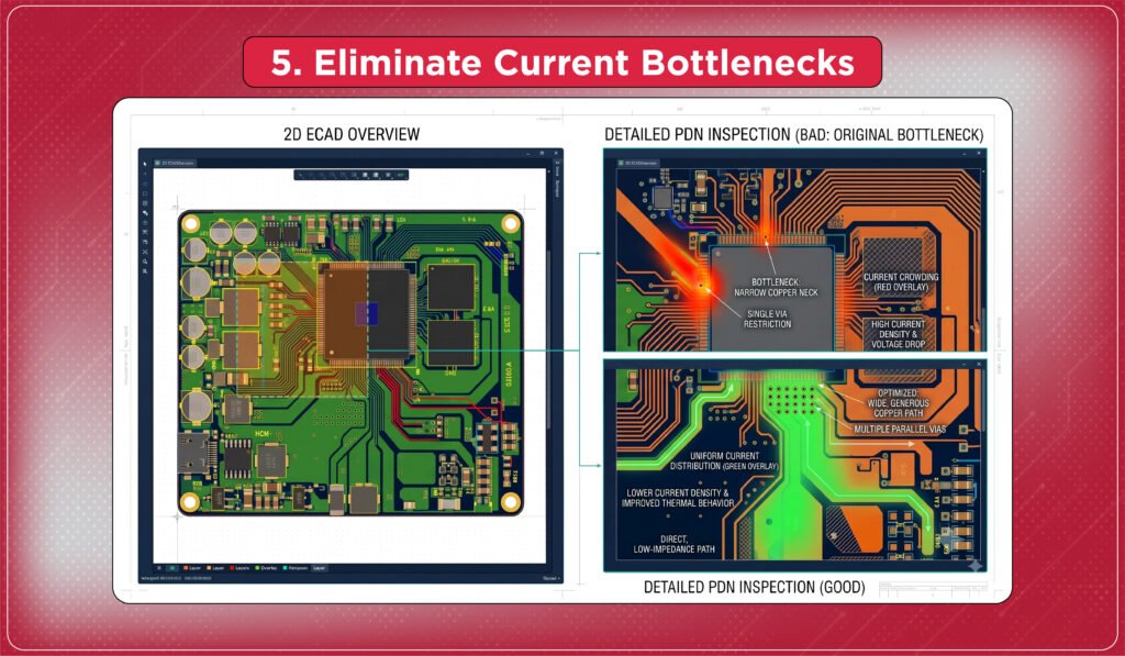
5. Eliminate Current Bottlenecks
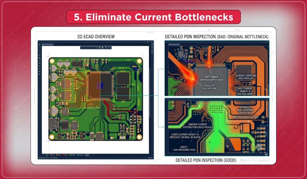
A large power plane can still fail if current must pass through narrow copper sections or a single via.
High-current devices such as processors and FPGAs should use generous copper widths and multiple vias to distribute current evenly. This reduces voltage drop, lowers current density, improves thermal performance, and enhances long-term reliability.
6. Validate Before Manufacturing

Layout review alone cannot reveal every power integrity issue.
Before fabrication, perform:
- Power Integrity (PI) Analysis
- DC IR Drop Analysis
- Current Density Analysis
- Thermal Analysis
These simulations identify excessive impedance, overloaded copper regions, voltage drop, and thermal hotspots before they become expensive prototype failures.
Real-World Power Plane Design Example
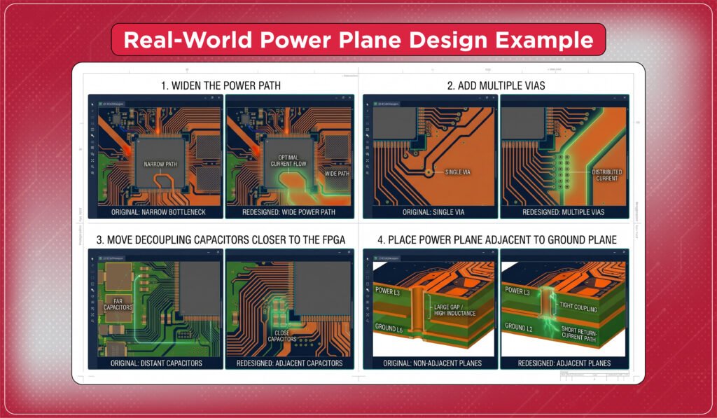
A networking PCB experienced intermittent FPGA resets whenever multiple high-speed interfaces operated simultaneously. Investigation revealed a narrow power-plane neck and a single via feeding the FPGA core voltage.
The design was updated by widening the power path, adding multiple vias, relocating decoupling capacitors closer to the FPGA, and placing the power plane adjacent to the ground plane.
The redesign reduced voltage ripple, eliminated unexpected resets, and improved EMI performance without changing the schematic—demonstrating that power integrity often depends more on layout than circuit design.
PCB Power Plane Checklist
Before releasing your PCB, verify that:
- Power and ground planes are continuous.
- High-current paths avoid copper bottlenecks.
- Decoupling capacitors are placed close to ICs.
- Multiple vias support high-current transitions.
- Return current paths remain uninterrupted.
- Power integrity and thermal analyses are complete.
Final Thought
An optimized PCB power plane design is essential for delivering clean, stable power to modern electronic systems.
By reducing PDN impedance, keeping power and ground planes closely coupled, optimizing decoupling, eliminating current bottlenecks, and validating the design through simulation, engineers can improve power integrity, reduce EMI, and minimize costly PCB re-spins.
Want to avoid hidden issues in your design?
Connect with us for the expert free consultation
https://calendly.com/gighz/30min
Stuck in a loop of challenges? Always pick smart solution that works
Have you faced costly rework because 2D drawings skipped in MCAD workflows?
Effective way to prevent MCAD documentation errors recalls?
Please answer both poll questions before submitting.
Thank you for your response! 😊
Latest Post
Get Customized Engineering CAD Design Service

Book a Free Consultation Call
Partner with Gighz and bring your most innovative design concepts to life. Our engineering cad services accelerate development so you can focus on your big vision.
