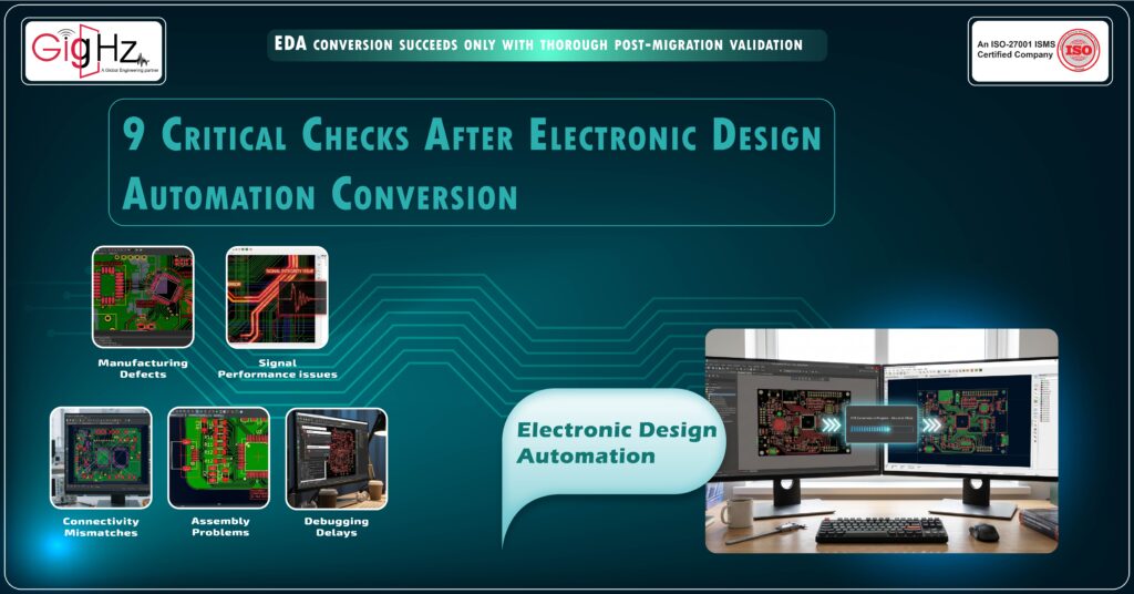
9 Critical Checks After Electronic Design Automation Conversion
- Posted On:
- June 8, 2026
- Category:
- Ecad
Design conversion is not just about opening a PCB file in another software tool.
In Electronic Design Automation workflows, migration must preserve electrical behaviour, routing logic, and manufacturing readiness.
Many engineers think the job is finished once the file opens successfully.
But in real engineering work, that is not true.
Small migration mistakes can create bigger problems later.
If conversion errors are ignored, teams may face:
- Manufacturing defects
• Signal performance issues
• Connectivity mismatches
• Assembly problems
• Debugging delays
Conversion is not just about moving files.
It is about making sure the design remains accurate and reliable.
Taking time to verify migration results can save weeks of redesign work and production cost.
Simple Checklist Before Conversion
- Keep backup of original files
- Export netlist data separately
- Save layer stack details
- Lock library versions
- Record design rule settings
- Collect BOM and schematic data
Skipping preparation can make debugging harder later.
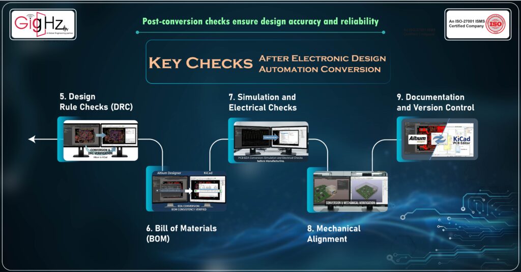
Key Checks After Electronic Design Automation Conversion
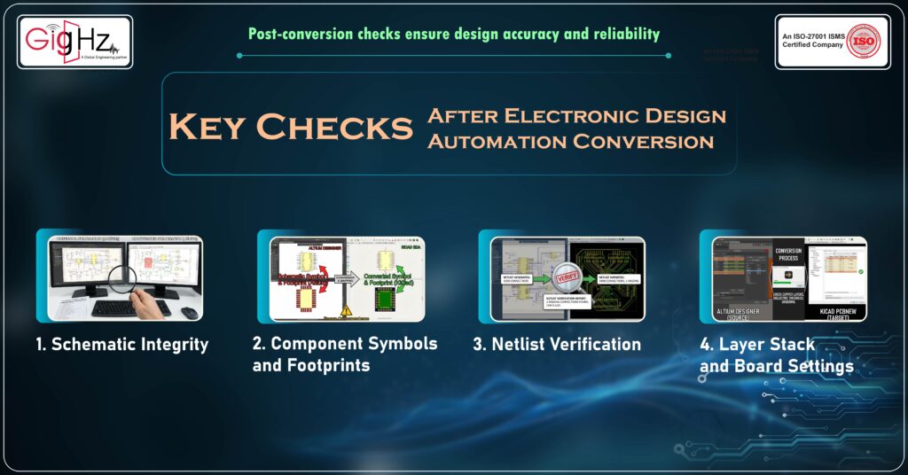
1. Schematic Integrity
After conversion, the schematic must exactly match the original design.
- Check for missing components or incorrect part numbers.
- Verify that connections are intact; even a single broken net can ruin a circuit.
- Confirm that reference designators (R1, C5, U3) remain unchanged.
- Automated tools may sometimes misinterpret hierarchical blocks, so manual inspection is critical.
Tip: Use a netlist comparison to quickly identify discrepancies.
2. Component Symbols and Footprints
Different EDA tools may use different libraries, which can cause symbol or footprint mismatches.
- Ensure that schematic symbols correspond to the correct PCB footprints.
- Verify pad sizes, pin numbers, and component orientation.
- Confirm proper component library mapping between the source and target tools.
- Watch for unmapped or generic components that may have been auto-assigned during migration.
Example: A microcontroller footprint may appear correct visually, but a pin swap can result in a non-functional board.
3. Net list Verification
The netlist is the backbone of your design and defines all electrical connections.
- Compare the converted netlist with the original to catch missing or extra connections.
- Pay special attention to power and ground nets, which are critical for circuit operation.
- Ensure signal paths remain accurate and no unintended shorts or opens appear.
Pro tip: Automated netlist comparison tools can quickly highlight differences.
4. Layer Stack and Board Settings
EDA conversion may sometimes reset or alter layer stack definitions.
- Check copper layers, dielectric thickness, and layer ordering.
- Confirm that drill sizes, vias, and board outlines are preserved.
- Reverify controlled impedance settings for high-speed signal layers.
Why it matters: A small change in layer thickness can affect signal integrity and impedance, leading to failures in high-speed PCB designs.
5. Design Rule Checks (DRC)
After conversion, always rerun the design rule checks in the target tool.
- Verify clearances, trace widths, and via-to-pad rules.
- Check copper spacing, minimum drill sizes, and board edge clearances.
- Run Electrical Rule Check (ERC) if supported by the EDA tool.
Insider tip: Even if the original design passed DRC, converted designs may fail due to unit or scale differences between tools.
6. Bill of Materials (BOM) Consistency
EDA conversion can alter part numbers, footprints, or supplier references.
- Verify that the Bill of Materials (BOM) is intact with correct component references.
- Check manufacturer part numbers (MPN) and supplier information.
- Look for duplicate entries, missing fields, or formatting changes.
Why it matters: Incorrect BOM data can delay procurement and increase project costs.
7. Simulation and Electrical Checks
Before manufacturing, verify the electrical behaviour of the converted design.
- Run circuit simulations such as SPICE where applicable.
- Perform signal integrity and power integrity checks for high-speed designs.
- Look for unexpected shorts, opens, or impedance mismatches.
Example: A schematic may convert successfully, but signal behaviour may change in high-speed circuits if routing parameters differ.
8. Mechanical Alignment
For boards with tight enclosures or connectors, verify the mechanical layout carefully.
- Check component placement relative to board edges.
- Confirm mounting holes, cut-outs, and board outline accuracy.
- Verify connector positions and orientations.
- Review 3D component models to ensure proper mechanical clearance.
Even small alignment errors can cause assembly problems, especially in multi-board systems.
9. Documentation and Version Control
Proper documentation is essential after conversion.
- Update version numbers and maintain change logs.
- Document any corrections made during the migration process.
- Keep both source and converted files for traceability.
- Regenerate manufacturing outputs such as Gerber files, drill files, and fabrication drawings.
Pro tip: Clear documentation helps teams avoid confusion when multiple engineers work on the same design.
What Happens If You Skip These Checks?
Skipping verification after Electronic Design Automation conversion can create hidden engineering risks.
If these checks are ignored, you may face:
- Manufacturing failures during fabrication
- Signal quality or routing performance problems
- Connectivity mismatches
- Power distribution instability
- Difficult debugging after production starts
Remember this simple engineering truth.
Conversion tools help move design data from one platform to another.
But only proper validation ensures the design works as intended.
Spending a little time on verification can prevent expensive redesigns and project delays later.
Final Thoughts
Electronic Design Automation conversion is not just file migration.
It is about keeping the design working the same way after moving to another tool.
Check rules carefully.
Verify connectivity.
Generate fresh manufacturing files.
Do a final visual review before release.
Small migration mistakes can create big production problems later.
Always remember that conversion is a checking and verification process, not just a file format change.
Good conversion means the design is reliable, manufacturing-ready, and performs as expected after migration.
Taking a little extra time for validation can save redesign effort and production delays in the future.
A few careful checks after conversion can protect the entire design from costly mistakes.
If you have questions or would like to discuss your project, feel free to contact us.
Book a Call. Schedule a Free Consultation now. https://calendly.com/gighz/30min
Stuck in a loop of challenges? Always pick smart solution that works
Have you faced costly rework because 2D drawings skipped in MCAD workflows?
Effective way to prevent MCAD documentation errors recalls?
Please answer both poll questions before submitting.
Thank you for your response! 😊
Latest Post
Get Customized Engineering CAD Design Service

Book a Free Consultation Call
Partner with Gighz and bring your most innovative design concepts to life. Our engineering cad services accelerate development so you can focus on your big vision.