Every electronic product starts with a schematic.
A schematic shows how components connect electrically. It explains how signals move, how power flows, and how the circuit functions.
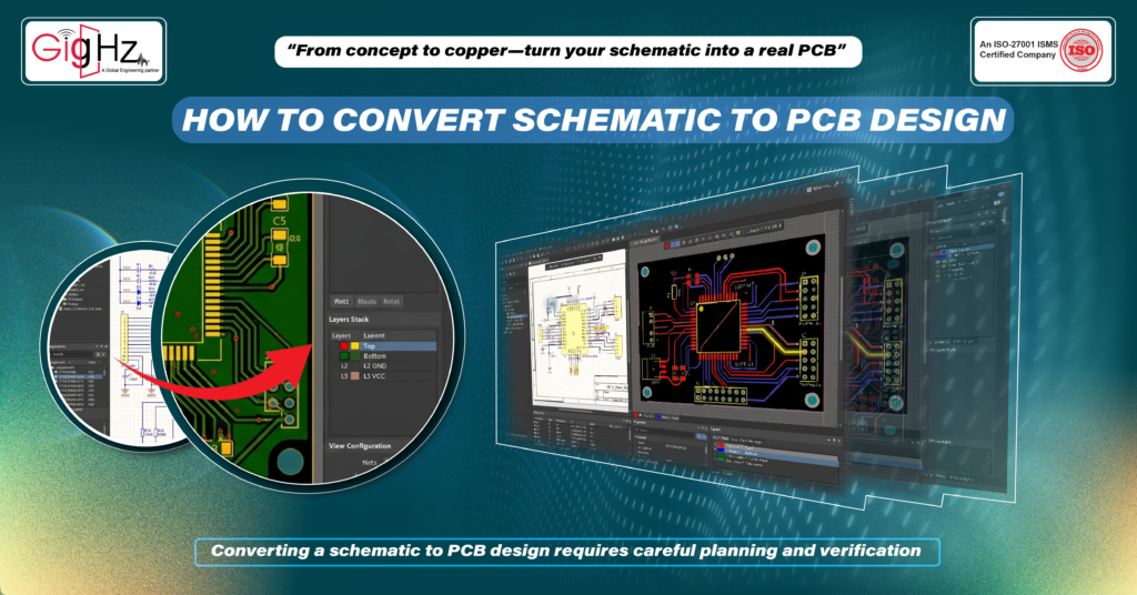
But a schematic alone cannot be manufactured.
To build a real electronic device, the schematic must be converted into a PCB design. This process defines where components are placed on the board and how copper traces connect them.
Converting a schematic to PCB design requires careful planning and verification. Following a structured process ensures the board works correctly and can be manufactured without issues.
Let’s walk through the practical steps involved.
Step-by-Step Process to Convert Schematic to PCB Design
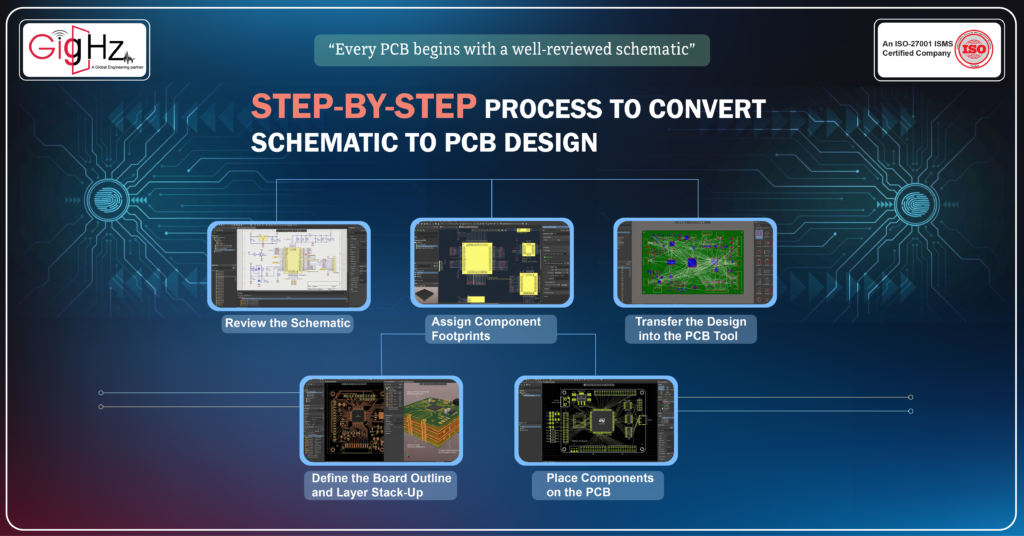
Review the Schematic
The first step is reviewing the schematic carefully.
Before starting PCB design, confirm that the circuit logic is correct.
Typical checks include:
- Confirming all components are connected properly
- Verifying power and ground connections
- Checking component values
- Ensuring each component has a footprint
Most Electronic Design Automation tools provide Electrical Rule Check (ERC) features. These checks help detect missing connections or incorrect pin relationships.
Fixing errors at the schematic stage prevents problems later in the design process.
Assign Component Footprints
Schematic symbols represent electrical functions. However, PCB design requires physical component packages.
This physical representation is called a footprint.
Footprints define:
- Pad locations
- Package dimensions
- Pin numbering
- Mounting type (SMD or through-hole)
For example, an integrated circuit may be available in packages like QFN, BGA, or TQFP.
Selecting the correct footprint ensures the component fits properly on the PCB and can be assembled during manufacturing.
Transfer the Design into the PCB Tool
After verifying the schematic and assigning footprints, the design is transferred into the PCB design environment.
Most EDA tools allow direct synchronization between schematic and PCB tools.
During this step:
- All components appear in the PCB workspace
- Electrical connections appear as connection lines
- Netlists define how components must connect
Initially, components may appear outside the board area. This is normal before placement begins.
Define the Board Outline and Layer Stack-Up
In the schematic to PCB design process, the next step is to define the physical structure of the PCB.
This includes the board outline and the layer stack-up.
The layer stack-up determines how copper and insulating layers are arranged within the board.
Important elements include:
- Number of copper layers
- Signal layers
- Ground and power planes
- Copper thickness
- Dielectric materials
Simple products often use two-layer PCBs, while more complex systems may use four or six layers.
Proper stack-up planning helps improve signal behavior, reduce noise, and support stable power distribution.
Place Components on the PCB
Component placement is a critical step in PCB design.
Typically, major components are placed first, such as processors, connectors, power devices, and large integrated circuits.
Once these are positioned, smaller supporting components such as resistors and capacitors are placed nearby.
Good placement practices include:
- Keeping signal paths short
- Placing decoupling capacitors close to IC power pins
- Grouping related circuits together
- Separating analog and digital sections when necessary
Careful placement helps simplify the next stage of PCB design.
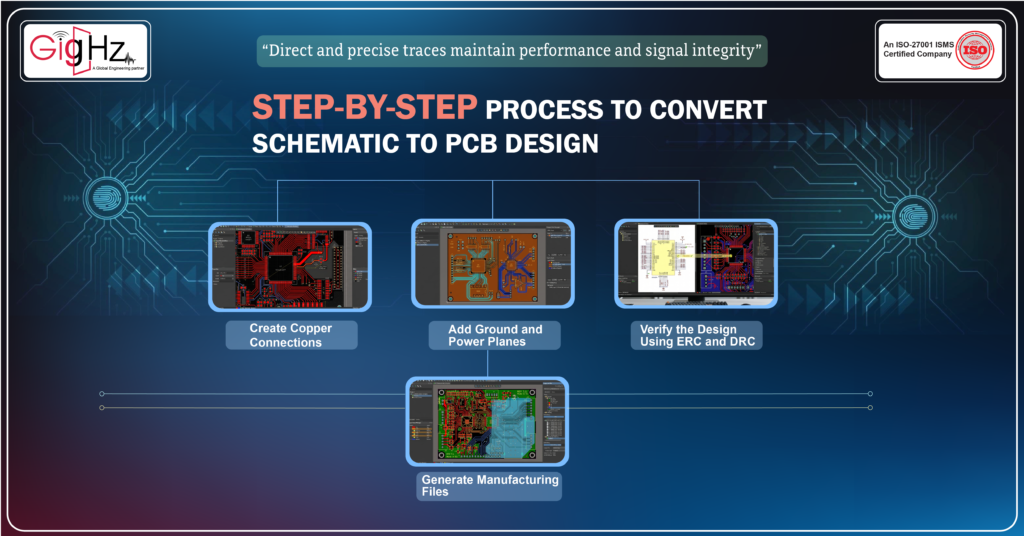
Create Copper Connections
After placement, the next stage in the schematic to PCB design process is creating copper traces to connect components
Each trace follows the netlist defined in the schematic.
Different signals require different approaches.
Power connections
Power traces must handle current safely. Designers often use wider traces or power planes.
Signal connections
Signal traces should be short and direct to maintain signal quality.
High-speed signals
High-speed circuits require controlled impedance and consistent spacing between differential pairs.
Although many tools support automatic routing, critical signals are often connected manually for better control.
Add Ground and Power Planes
Ground plays an important role in PCB performance.
Instead of connecting ground through individual traces, designers usually create solid ground planes.
Ground planes provide several advantages:
- Stable current return paths
- Reduced electrical noise
- Improved signal integrity
- Better thermal performance
Power planes help distribute voltage evenly across the board.
In mixed-signal designs, careful ground management prevents digital noise from affecting analog circuits.
Verify the Design Using ERC and DRC
Before manufacturing, verify the design using ERC and DRC checks.
Electrical Rule Check (ERC) – performed during the schematic stage
- Detects missing connections
- Identifies incorrect pin types
- Finds unconnected power or ground pins
- Ensures circuit logic is correct
Design Rule Check (DRC) – performed after creating the PCB design
- Verifies minimum trace width
- Checks spacing between copper traces
- Confirms via and drill size limits
- Ensures the PCB follows manufacturing rules
Running these checks helps identify errors before fabrication.
Generate Manufacturing Files
After the PCB design passes verification, the final step is generating manufacturing data.
Design tools produce standard files required for fabrication and assembly.
Common outputs include:
- Gerber files for PCB layers
- Drill files for holes and vias
- Bill of Materials (BOM)
- Pick-and-place files for automated assembly
These files allow manufacturers to fabricate and assemble the PCB accurately.
At this stage, the schematic has successfully been converted into a real PCB ready for production.
Final Thoughts
Converting a schematic to PCB design is an essential step in electronic product development.
It transforms a circuit concept into a physical board that can be manufactured and tested.
The process involves verifying the schematic, selecting correct footprints, planning the layer stack-up, placing components carefully, and validating the design using ERC and DRC checks.
Each step plays a critical role in ensuring the PCB functions correctly and meets manufacturing requirements.
A well-executed schematic to PCB process helps reduce design errors, improve signal reliability, and support efficient production.
Understanding this workflow improves design accuracy and ensures PCBs perform reliably in real-world applications.
Have a project in mind?
Contact us to learn how our team can support your engineering design needs.
Book a Call. Schedule a Free Consultation now. https://calendly.com/gighz/30min
Stuck in a loop of challenges? Always pick smart solution that works
Have you faced costly rework because 2D drawings skipped in MCAD workflows?
Effective way to prevent MCAD documentation errors recalls?
Please answer both poll questions before submitting.
Thank you for your response! 😊
Latest Post
Get Customized Engineering CAD Design Service

Book a Free Consultation Call
Partner with Gighz and bring your most innovative design concepts to life. Our engineering cad services accelerate development so you can focus on your big vision.