7 Essential Design Considerations for Mixed-Signal PCB Layout
- Posted On:
- June 4, 2026
- Category:
- Ecad
What if a PCB design looks perfect during bench testing but later shows noise spikes, unstable readings, or communication glitches after deployment?
Many hardware engineers face this real-world problem.
In theory, everything may look correct.
Clean schematic.
Passing routing rules.
Early testing may appear successful.
But electronics behave differently in continuous real operating environments.
Most hardware failures do not appear suddenly.
They usually start quietly from small layout decisions made during early development.
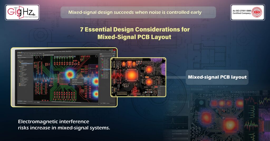
As electronic devices become smaller and faster, thermal density, routing complexity, and electromagnetic interference risks increase in mixed-signal systems.
The real challenge appears when precision analog circuits and high-speed digital switching networks share the same PCB.
At this level, design is not only about functionality.
It is about stability, noise control, and predictable long-term performance.
Mixed-signal PCB layout must be treated as a system-level engineering process.
The design process begins by understanding signal behavior across PCB regions.
Core Engineering Guidelines for Reliable Mixed-Signal PCB Layout
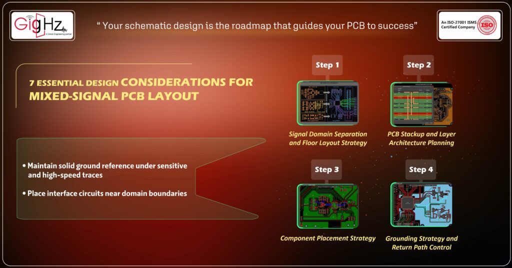
1. Signal Domain Separation and Floor Layout Strategy
When designing a mixed-signal PCB layout, the first priority is understanding how analog and digital circuits interact on the board.
Best practices include:
- Separating analog and digital regions on the PCB floorplan
• Placing ADCs or DACs at domain boundaries
• Grouping functional blocks according to signal function
• Avoiding random component placement
Boundary placement ensures signals move in a controlled direction across the board.
2. PCB Stackup and Layer Architecture Planning
After defining analog and digital domains, stackup planning determines signal behavior inside the board.
In this, layer structure directly affects impedance control, return paths, and EMI performance.
Key guidelines include:
- Place signal layers adjacent to solid ground planes
• Avoid routing across split reference planes
• Define impedance during stackup planning
• Maintain continuous reference for analog stability
A well-planned stackup forms the electrical foundation for reliable mixed-signal performance.
3. Component Placement Strategy
In mixed-signal PCB layout design, component placement plays a critical role in signal isolation, routing quality, and noise control.
For analog sections:
- Keep sensor interfaces, amplification stages, and ADC inputs close
- Use short, shielded traces for low-amplitude signals
- Avoid placing switching regulators near precision circuits
For digital sections:
- Group microcontroller, memory, and communication blocks together
- Keep clock circuits compact and isolated
- Avoid routing digital signals through analog zones
Simple rule: Short analog signal paths reduce noise sensitivity, while compact digital grouping helps reduce EMI radiation.
4. Grounding Strategy and Return Path Control
Grounding often decides whether a signal will behave predictably or become difficult to debug during testing and deployment.
The modern engineering approach is to use a continuous ground plane for most mixed-signal boards. Return current flows directly underneath signal traces along the path of least impedance rather than following schematic wiring paths.
Key practical guidelines:
- Maintain solid ground reference under sensitive and high-speed traces
• Place interface circuits near domain boundaries
• Use single-point connection for analog and digital ground separation
• Avoid routing critical signals across ground plane splits
• Minimize signal return loop area
Random ground splitting can increase noise coupling between analog and digital domains. If separation is necessary, connect analog and digital ground at a single reference point, usually near the ADC region.
5. Power Distribution and Noise Isolation
Stable power delivery is one of the silent foundations of reliable mixed-signal hardware.
Switching circuits, processors, and communication modules generate electrical noise that can propagate through power networks if not properly controlled.
Engineering practices include:
- Using separate regulators for analog and digital sections
• Adding ferrite bead filtering between noisy and sensitive power domains
• Placing decoupling capacitors close to IC power pins
• Using multiple capacitor values to suppress different noise frequencies
Minimizing current loop area helps reduce electromagnetic interference (EMI) and improves power integrity. A well-designed power network prevents instability, resets, and signal distortion in mixed-signal systems.
6. High-Speed Signal and Clock Management
High-speed signals behave differently from low-frequency circuits, and treating them like normal wires is a common design mistake.
If impedance matching is not controlled, signal reflections can occur, causing ringing, jitter, and waveform distortion.
To maintain signal quality:
- Route differential pairs symmetrically
• Match trace lengths for timing-critical signals
• Avoid sharp trace corners
• Maintain solid ground reference under high-speed traces
Clock networks require special care because they are major internal noise sources.
Keep clock routing short and isolated from analog input paths.
7. EMI Risk Analysis and Design Validation
Verification is where theoretical design meets real hardware behavior.
Important analysis methods include:
- Thermal simulation to monitor heat distribution
• Signal integrity analysis for high-speed paths
• Power integrity analysis under dynamic load conditions
• EMI and EMC risk evaluation during layout review
• Mechanical stress assessment for vibration-sensitive systems
Early verification helps identify hidden weaknesses before manufacturing.
Engineering confidence should always come from measurable design data rather than assumptions.
Why Mixed-Signal PCB Design Matters
Mixed-signal PCB layout design ensures predictable hardware behavior across operating environments.
It is not only about routing correctness but about building systems that maintain stability under real-world electrical, thermal, and mechanical stress.
Mixed-signal hardware is widely used in embedded electronics, communication modules, medical instruments, and industrial automation systems where signal accuracy and continuous operation are critical.
Key reliability factors include:
- Thermal balance across component regions
• Clean signal transmission paths
• Stable low-noise power networks
• Effective EMI suppression
• Environmental durability
As devices become more compact and high-performance, design tolerance margins shrink.
A single layout decision can influence product behavior long after deployment.
That is why reliability engineering should be integrated from the earliest design stage.
Final Thoughts
What if hardware reliability could be improved by simply thinking deeper about how signals behave inside the system?
Engineering design is about understanding system behavior — not just following layout rules.
Mixed-signal PCB layout design is not only about separating analog and digital circuits.
It is about controlling how currents, signals, and noise interact inside the hardware structure.
Good engineering comes from disciplined placement, controlled routing, and systematic validation.
- Thermal imbalance can shorten component life.
- Signal integrity problems can create intermittent failures.
- Weak power distribution can silently reduce product reliability.
Reliability engineering is not something added at the end.
It is a design philosophy that must be embedded in every routing decision, stackup choice, and verification step.
If your product cannot tolerate unexpected field failures, reliability must be planned from the very beginning.
If you would like to discuss your PCB design requirements, feel free to contact our team.
Book a Call. Schedule a Free Consultation now. https://calendly.com/gighz/30min
Stuck in a loop of challenges? Always pick smart solution that works
Have you faced costly rework because 2D drawings skipped in MCAD workflows?
Effective way to prevent MCAD documentation errors recalls?
Please answer both poll questions before submitting.
Thank you for your response! 😊
Latest Post
Get Customized Engineering CAD Design Service

Book a Free Consultation Call
Partner with Gighz and bring your most innovative design concepts to life. Our engineering cad services accelerate development so you can focus on your big vision.