


Let’s be honest.
Every PCB designer has experienced this moment:
The board is routed. It looks clean. Tracks are neat. Silkscreen is beautiful.
You generate Gerbers… send them to fabrication… and then…
“Minimum clearance violation.”
“Unconnected net.”
“Drill-to-copper too close.”
And suddenly your “perfect” board isn’t perfect.
That’s exactly why Design Rule Check (DRC) exists.
DRC in PCB Design
A Design Rule Check (DRC) is an automated verification process inside PCB design tools (like Altium Designer, KiCad, or Cadence Allegro) that ensures your layout follows:
- Manufacturing constraints
- Electrical safety rules
- Spacing and clearance standards
- Company or project-specific design guidelines
Think of DRC as your silent manufacturing engineer sitting beside you, checking every track you draw.
Why DRC is Not Optional
Skipping DRC is like skipping a spell check in a legal contract.
Here’s what DRC prevents:
- Short circuits between traces
- Open circuits (missing connections)
- Fabrication rejection
- Assembly failures
- EMI issues due to spacing errors
- Drill breakouts
- Solder mask misalignment
If you want a first-pass success PCB, DRC is mandatory.
Step-by-Step: How to Perform a DRC Properly
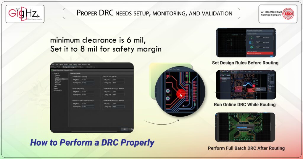
Let’s walk through it the right way — not just clicking “Run DRC” at the end.
Step 1: Set Design Rules Before Routing
This is where most beginners go wrong.
Never start routing without defining rules.
Configure:
Clearance Rules
- Trace-to-trace spacing
- Trace-to-pad spacing
- Via-to-via spacing
- Copper-to-board-edge clearance
Example:
If your manufacturer says minimum clearance is 6 mil, set it to 8 mil for safety margin.
Trace Width Rules
Define minimum and preferred widths.
- Signal traces (e.g., 6–8 mil)
- Power traces (calculated based on current)
- High-speed differential pairs (controlled impedance)
Via Rules
- Minimum drill size
- Annular ring size
- Via-to-via clearance
Example:
0.3 mm drill with 0.6 mm pad = 0.15 mm annular ring.
Plane & Polygon Rules
- Minimum copper-to-copper clearance
- Thermal relief connection style
- Minimum polygon neck width
Differential Pair Rules (If High-Speed)
- Gap between pairs
- Matched length tolerance
- Maximum skew
Step 2: Run Online DRC While Routing
Modern tools allow real-time DRC.
Enable online rule checking.
When you route:
- If spacing is violated → tool shows red marker
- If width is wrong → warning pops up
- If copper overlaps → error flag appears
This prevents accumulation of 200+ errors at the end.
Step 3: Perform Full Batch DRC After Routing
Once routing is complete:
- Save your design
- Run full DRC
- Generate DRC report
Now analyze errors carefully.
Understanding Common DRC Errors (And How to Fix Them)
Let’s decode what they actually mean.
Clearance Violation
Two copper objects are too close.
Fix:
- Move trace
- Reduce width
- Adjust rule (only if allowed)
Unconnected Net
A pin is not electrically connected.
Fix:
- Re-route missing trace
- Check net assignment
- Verify schematic-to-PCB sync
Drill-to-Copper Violation
Via hole too close to copper region.
Fix:
- Increase spacing
- Reduce via size
- Modify plane clearance rule
Solder Mask Sliver Error
Tiny strip of solder mask between pads.
Fix:
- Increase mask expansion
- Merge mask openings
Silkscreen Over Pad
Text or reference designator overlapping pad.
Fix:
- Move silkscreen
- Resize text
Advanced DRC Checks Professionals Use
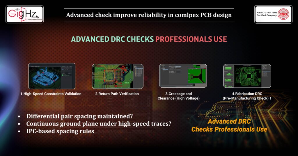
Now let’s go deeper — because basic DRC is not enough for complex boards.
High-Speed Constraints Validation
- Differential pair spacing maintained?
- Length matching within tolerance?
- Impedance rules applied correctly?
Return Path Verification
Even if DRC passes spacing rules,
Check:
- Is there a continuous ground plane under high-speed traces?
- Any split plane crossing?
DRC may not detect signal integrity risks unless specifically configured.
Creepage and Clearance (High Voltage)
For power electronics:
- IPC-based spacing rules
- Pollution degree-based constraints
These must be manually configured.
Fabrication DRC (Pre-Manufacturing Check)
Before sending Gerbers:
- Minimum drill size compatible?
- Annular ring sufficient?
- Copper-to-edge rule satisfied?
- Panelization clearance verified?
Many designers also upload Gerbers to manufacturers like JLCPCB or PCB Way to run their automated DFM checks.
When Should You Run DRC?
Best Practice Timeline:
- After component placement
- After power routing
- After high-speed routing
- Before polygon pour
- After final routing
- Before Gerber generation
Never run it only once at the end.
Pro Tips for Zero-Debug PCB
Use stricter rules than manufacturer minimums
Margin = reliability.
Separate rules by net class
- Power nets
- High-speed nets
- Analog nets
- Standard signal nets
Fix errors, don’t suppress them
Suppressing errors = hiding a future failure.
Keep DRC report clean before release
Zero critical errors.
Zero unconnected nets.
Warnings? Review carefully.
Final Checklist Before Sending to Fabrication
Ask yourself:
- Does DRC show 0 errors?
- Are all nets connected?
- Is solder mask correct?
- Are drill sizes validated?
- Is silkscreen readable?
- Is board outline correct?
- Are mounting holes plated/non-plated correctly defined?
If yes — now you’re ready.
Final Thoughts
DRC is not just a button.
It is a discipline.
The difference between:
- A board that works first time
vs - A board that needs 3 re-spins
Usually lies in how seriously DRC was taken.
Design beautifully.
But verify ruthlessly.
And if you want your next PCB to pass manufacturing the first time —
Planning your next PCB design?
Connect with our engineering team for reliable design support
Book a Call. Schedule a Free Consultation now. https://calendly.com/gighz/30min
Stuck in a loop of challenges? Always pick smart solution that works
Have you faced costly rework because 2D drawings skipped in MCAD workflows?
Effective way to prevent MCAD documentation errors recalls?
Please answer both poll questions before submitting.
Thank you for your response! 😊
Latest Post
Get Customized Engineering CAD Design Service

Book a Free Consultation Call
Partner with Gighz and bring your most innovative design concepts to life. Our engineering cad services accelerate development so you can focus on your big vision.
