Let’s start with a reality check.
If your mixed-signal board shows unstable ADC readings, unexpected noise, random EMI failures, or inconsistent lab results —
there’s a high chance the problem is not your firmware.
It’s your layout.
Mixed-signal PCB design is not about keeping analog on the left and digital on the right.
It’s about controlling how noise moves.
Let’s break it down practically and technically.
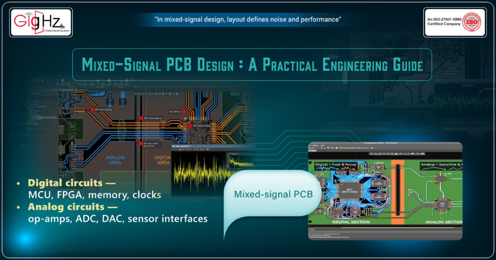
Understanding Mixed-Signal PCB Design
A mixed-signal PCB contains both:
- Digital circuits — MCU, FPGA, memory, clocks
- Analog circuits — op-amps, ADC, DAC, sensor interfaces
Digital circuits switch fast.
Analog circuits measure tiny voltages.
Digital is loud.
Analog is sensitive.
Your job as a PCB designer is to let them coexist — without interference.
Why Mixed-Signal Boards Fail in Real Projects
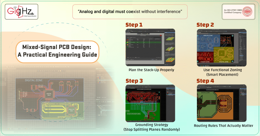
Step 1: Plan the Stack-Up Properly
Before opening tools like Altium Designer or KiCad, define the stack-up.
For most mixed-signal boards, use at least a 4-layer structure:
Layer 1 – Signals
Layer 2 – Solid Ground Plane
Layer 3 – Power Plane
Layer 4 – Signals
Why?
Because a continuous ground plane ensures controlled return current.
If return current is uncontrolled, noise spreads.
Never design mixed-signal boards without a solid reference plane.
Step 2: Use Functional Zoning (Smart Placement)
This is the most important stage.
Divide the board logically:
Analog Zone
- ADC
- Op-amps
- Reference circuits
- Sensor inputs
Digital Zone
- MCU
- Memory
- Clock circuits
- Communication interfaces
Power Zone
- Switching regulators
- Linear regulators
- Power filters
Now here’s the key:
Separate by function — not by random physical gaps.
Keep analog components close together.
Keep digital components clustered.
Keep switching power circuits away from analog inputs.
Placement controls noise before routing even begins.
Step 3: Grounding Strategy (Stop Splitting Planes Randomly)
This topic causes confusion everywhere.
Should you split analog and digital ground?
In modern PCB design — usually no.
Instead:
- Use one continuous ground plane.
- Keep return paths short.
- Control routing so digital currents don’t flow through analog areas.
If you split planes incorrectly:
- Return current detours
- EMI increases
- Signal integrity degrades
The goal is not physical separation —
it’s return current control.
Step 4: Routing Rules That Actually Matter
Routing discipline is one of the most critical factors in reliable mixed-signal PCB design.
Now let’s get practical.
Rule 1: Never Route Digital Signals Through Analog Zone
Digital signals carry fast edges.
Fast edges generate noise.
If routed near ADC inputs, they inject interference.
Keep digital routing inside digital zone.
Rule 2: Protect ADC Reference Lines
ADC reference is extremely sensitive.
- Keep reference trace short
- Avoid running it parallel to digital traces
- Shield with ground where possible
- Avoid vias if you can
A noisy reference = inaccurate measurement.
Rule 3: Keep Clock Lines Contained
Clock signals are strong noise sources.
- Route them short
- Avoid crossing analog sections
- Avoid running them over plane splits
- Surround with ground when possible
Treat clocks like controlled high-frequency signals.
Rule 4: Separate Analog and Digital Power
Even if ground is common, power should be filtered.
Use:
- Ferrite beads between AVDD and DVDD
- Separate decoupling networks
- LC filters for analog rails
For example:
DVDD → Digital logic
AVDD → ADC + analog front end
Filtered properly.
Step 5: Decoupling Is Not Optional
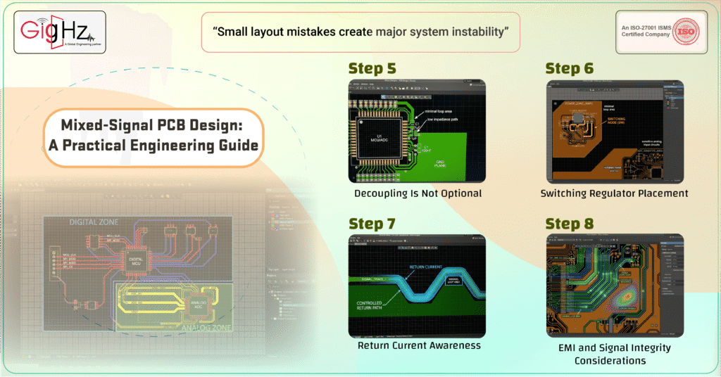
Every IC must have proper bypass capacitors.
For mixed-signal ICs:
- Place decoupling capacitors close to pins
- Direct via to ground plane
- Use multiple values (100nF + 1µF typical combination)
Poor decoupling creates noise injection paths.
Step 6: Switching Regulator Placement
Switching regulators are high-noise devices.
If using SMPS:
- Keep switching loop area small
- Place far from analog input circuits
- Do not route sensitive signals near inductor
Switching node = strongest noise source on the board.
Keep it isolated.
Step 7: Return Current Awareness
Current always returns under the trace.
If a digital trace crosses a split or void:
- Return current spreads.
- Loop area increases.
- EMI increases.
Keep signal and reference plane continuous.
Never route over gaps in ground.
Step 8: EMI and Signal Integrity Considerations
Mixed-signal boards often fail EMI tests because:
- Loop areas are large
- Return paths are broken
- High-speed edges are uncontrolled
Reduce EMI by:
- Minimizing loop area
- Using solid ground plane
- Controlling trace impedance
- Keeping fast edges short
If clock > 50 MHz, treat routing seriously.
Real-World Example
Suppose you have:
- 100 MHz MCU
- 16-bit ADC
- Temperature sensor
- Switching regulator
Poor design:
- SMPS placed near ADC
- Clock routed across analog input
- Long reference trace
- Split ground plane
Result:
ADC noise ±15 LSB.
Improved design:
- Proper zoning
- Solid ground
- Filtered AVDD
- Short reference routing
- Clock isolated
Result:
Stable readings within ±1 LSB.
Same components.
Different layout discipline.
Common Mixed-Signal Mistakes
- Splitting ground plane without understanding return path
- Long analog traces
- Routing clock near sensor input
- Poor decoupling placement
- Ignoring switching loop placement
- Crossing plane gaps
Most mixed-signal failures are predictable.
Final Engineering Checklist
Before generating Gerbers:
- Is ground plane continuous?
- Are analog and digital zones clearly defined?
- Are clock lines isolated?
- Are ADC reference traces short?
- Are decoupling capacitors properly placed?
- Are switching regulators isolated from analog?
If all are yes — your board is engineered, not just drawn.
Final Thoughts
Mixed-signal PCB design is not about separating analog and digital physically.
It is about:
Managing return currents.
Controlling noise paths.
Designing with discipline.
Digital circuits create noise.
Analog circuits measure reality.
Your layout decides whether they cooperate — or fight.
Looking for engineering support? Connect with our team.
Need technical guidance? Contact Our Engineering Team
https://gighz.net/contact-us/
Book a Call. Schedule a Free Consultation now. https://calendly.com/gighz/30min
Stuck in a loop of challenges? Always pick smart solution that works
Have you faced costly rework because 2D drawings skipped in MCAD workflows?
Effective way to prevent MCAD documentation errors recalls?
Please answer both poll questions before submitting.
Thank you for your response! 😊
Latest Post
Get Customized Engineering CAD Design Service

Book a Free Consultation Call
Partner with Gighz and bring your most innovative design concepts to life. Our engineering cad services accelerate development so you can focus on your big vision.