PCB Design Steps
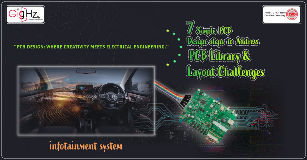
As you enjoy a relaxing evening drive, taking in the lush green scenery and witnessing a beautiful sunrise through the car window, imagine listening to your favorite music on the road.
All of this is made possible through the infotainment system, with a silent helper at its core—the printed circuit board.
This little marvel quietly powers everything, ensuring that your music plays smoothly and that all the features work seamlessly, creating a pleasant and enjoyable driving experience.
When you’re in the midst of designing Printed Circuit Boards (PCBs), you’re likely to face some challenges along the way.
But fear not!
Recognizing the significance of PCBs and following a few simple steps can help you tackle these obstacles head-on.
PCBs are like the unsung heroes of electronic devices, connecting all the components and making everything work seamlessly.
By understanding the importance of PCBs and sticking to straightforward design methods, you can conquer those design challenges and craft efficient and dependable circuit boards with ease.
Let’s dig in!
Importance of PCB Design
Printed circuit board (PCB) design is a crucial aspect of the circuit design process.
A successful PCB layout ensures that the printed circuit board functions as intended, while meeting design rules and constraints. The layout design not only impacts the overall functionality of the circuit board, but also affects the PCB manufacturing process.
When designing your PCB, it is essential to consider the layout guidelines and design rules and constraints to ensure that the pcb layout meets the required specifications. Using pcb design software and conducting a design rule check can help pcb designers optimize the design process and produce a high-quality pcb circuit board.
When designing a PCB layout, it is important to go through the necessary design steps to produce a reliable Circuit board layout.
From schematic design to pcb design layout and pcb assembly, each step plays a crucial role in the design process.
The entire PCB must be taken into consideration during the layout process, including the size and shape of the PCB and the placement of pcb components.
By following a guide to pcb layout design and collaborating with a reputable pcb manufacturer or pcb supplier, pcb designers can ensure that their pcb board meets industry standards and is optimized for pcb assembly.
7 Simple PCB Design steps to Address PCB Layout Challenges
Let’s share an experience to illustrate how we tackled challenges and successfully navigated through the process of designing the display control board for a car’s infotainment system.
By outlining the steps we took and the strategies we implemented, we were able to overcome obstacles and achieve our goals effectively in enhancing the display controller board functionality within the vehicle’s infotainment setup
Step 1: Component reference designators
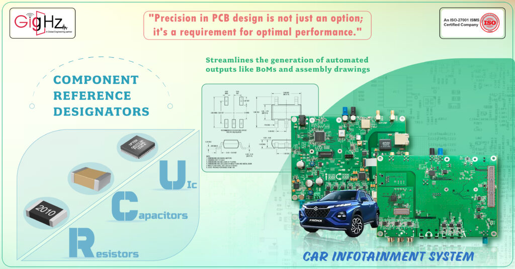
When it comes to component reference designators, it’s crucial to maintain a uniform and standardized approach across various aspects of the design process, including schematics, PCB layouts, Bills of Materials (BoMs), assembly drawings, and documentation.
Following common naming conventions such as using
“R” for resistors (e.g., R1, R2, R3),
“C” for capacitors (e.g., C1, C2, C3), and
“U” for integrated circuits (e.g., U1, U2, U3) offers several benefits:
- Promotes consistency across all design documentation and manufacturing stages.
- Helps prevent errors and discrepancies when transferring designs.
- Streamlines the generation of automated outputs like BoMs and assembly drawings.
- Simplifies manufacturability analysis and component procurement processes.
By adhering to standardized reference designators, you ensure a smoother design workflow, reduce the likelihood of mistakes, and facilitate efficient manufacturing processes.
Step 2: Grouping Components with Logical Prefixes and Parameterizing the Components for Flexibility
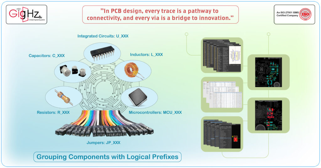
Grouping Components with Logical Prefixes
To enhance component organization, classify components into distinct groups using designated prefixes:
- Resistors: R_XXX
- Capacitors: C_XXX
- Integrated Circuits: U_XXX
- Inductors: L_XXX
- Test Points: TP_XXX
- Jumpers: JP_XXX Additional subgroups for specialized components:
- Power components: PC_XXX
- Interface ICs: UI_XXX
- Microcontrollers: MCU_XXX
“What will be the advantages of implementing these strategies?”
By structuring components with specific prefixes and logical grouping:
Enhanced Component Recognition: Improves the ease of identifying different component types.
Efficient Data Analysis: Streamlines sorting and filtering processes in data reports and analyses.
Simplified Layout Planning: Facilitates easier PCB layout floorplanning and zoning decisions.
Consistency Across Projects: Ensures a uniform design structure, fostering coherence in various
projects.
Parameterizing the Components for Flexibility
Employing parameters to specify component characteristics such as reference designator, value, package, rating, tolerance, and more provides numerous advantages:
Enhanced Property Modification: Simplifies property adjustments through a singular parameter change, facilitating easier editing.
Promoting Design Reusability: Enables the reuse of designs by updating instance properties, fostering efficiency in design iterations.
Supporting Design Variability: Allows for the creation of diverse design variants using parameter sweeps, enhancing flexibility in design exploration.
Streamlining BoM Generation: Facilitates the automated generation of Bills of Materials and seamless data transfer processes, optimizing production workflows and documentation management.
Step 3: Datasheet Organization
When structuring component datasheets consistently, it is vital to incorporate dedicated sections for essential data points to ensure clarity and ease of reference.
- Manufacturer Part Number
- Component Description
- Package Type
- Rating Specifications
- Operating Parameters
- Key Dimensions
- Recommended PCB Layout
- Special Notes
Here you will gain,
Comprehensive Data Capture: Ensures critical information is systematically documented in a standardized manner.
Facilitates Comparison and Review: Simplifies the process of comparing and reviewing component details for better decision-making.
Simplified Component Library Creation: Streamlines the creation and maintenance of component libraries for efficient design processes.
Facilitates Automated Parameter Extraction: Enables scripted extraction of key parameters, enhancing data retrieval and analysis capabilities.
Step 4: 3D Component Model Creation and Defining Net Names
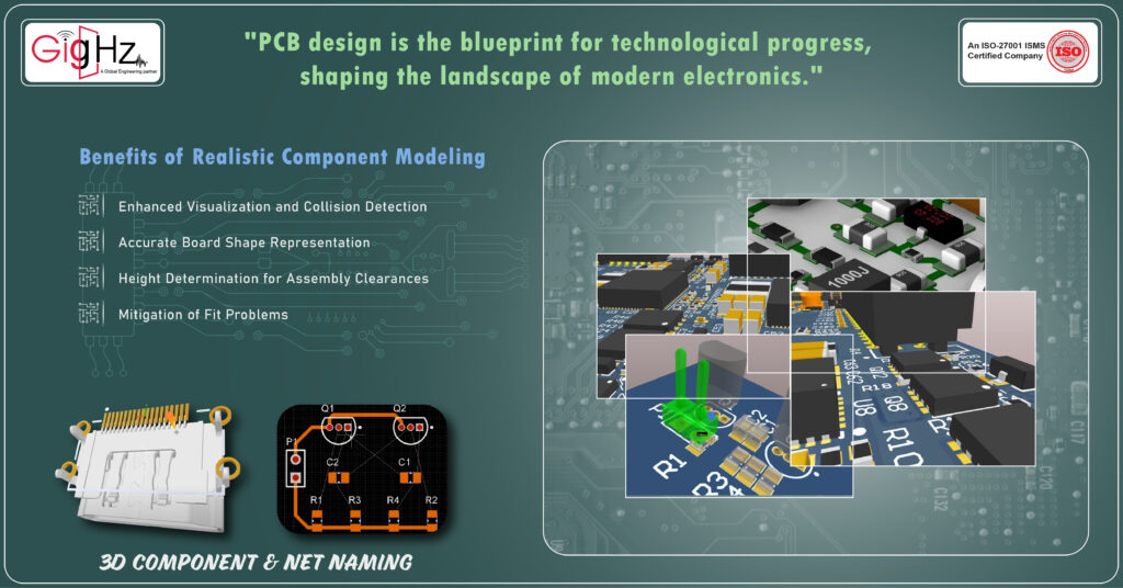
Crafting 3D component models that mirror real-life packages involves meticulous attention to detail:
- Accurate Dimension Representation
- Inclusion of Special Features like Tabs and Heatsinks
- Alignment of Model Orientation with Datasheet References
- Validation through Sample Inspection for Precision Verification
Benefits of Realistic Component Modeling:
Enhanced Visualization and Collision Detection: Facilitates realistic
rendering and precise collision assessment in design simulations.
Accurate Board Shape Representation: Ensures faithful portrayal of board geometry for enclosure fitting and overall design coherence.
Height Determination for Assembly Clearances: Enables precise height calculations crucial for avoiding clearance issues during assembly.
Mitigation of Fit Problems: Reduces the likelihood of fit-related challenges during prototyping and manufacturing stages.
Implementation of Descriptive Net Names and Classes
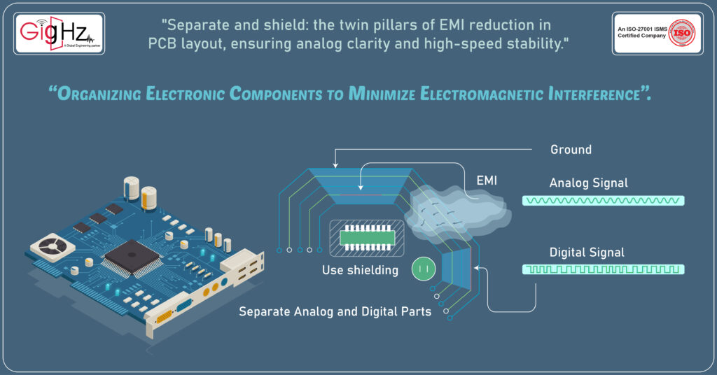
Assigning descriptive net names that indicate signal functions or ports and defining net classes for key groups like ANALOG, POWER, GROUND, DIGITAL, HIGH_SPEED, and ESD offers significant advantages:
Benefits of Net Naming and Classification:
Enhanced Signal Connection Clarification: Provides clear indications of signal paths and circuit functionality on schematics.
Facilitated PCB Trace Routing: Streamlines the process of routing traces and planning layers for different net categories.
Automated EMC/Signal Integrity Analysis: Allows for automated analysis based on net classes, enhancing EMC and signal integrity evaluations.
Simplified Wire Harness Generation: Aids in generating wire harnesses, test points, and assembly drawings efficiently, optimizing production processes.
Step 5: Padstack Creation and PCB Layout Restriction
Custom Padstack Creation for Varied Landing Patterns
Tailor unique padstack definitions to match the specific requirements of each component landing pattern configuration:
- Pad Size, Shape, and Offset
- Soldermask Cutouts
- Thermal Reliefs
- Hole SizesBenefits of Individualized Padstack Development:
Precision in Pad Modeling: Facilitates precise modeling of pad shapes necessary for different components.
Flexibility in Geometry Adjustments: Allows for easy modification of pad geometries by adjusting the padstack.
Automated Validation of Assembly Needs: Enables automated validation of padstack assembly requirements, streamlining the design validation process.
Mitigation of Footprint Assignment Errors: Reduces the risk of incorrect footprint assignments, ensuring accuracy in component placement.
Establishment of PCB Layout Restricted Areas
Define specific mechanical and assembly keep out areas to maintain design integrity:
- Exclusion Zones for Component Placement
- Board Outlines and Edges
- Locations of Mounting Holes
- Cutouts for Connectors, Switches, and Shielding
- Zones for Heat Sinks and Fans
Advantages of Restricted Area Definition:
Early Reservation of Mechanical Space: Reserves necessary space for mechanical features at the initial design stage.
Accurate Representation of Assembly Constraints: Ensures precise modeling of assembly restrictions for efficient manufacturing processes.
Respect for Critical Zones: Guarantees that critical areas such as mounting holes are appropriately acknowledged and accounted for.
Reduction of Late-Stage Iterations: Minimizes costly layout revisions later in the design cycle, optimizing the overall design process.
Step 6: Precision Board Outline Generation
Generate precise board outlines for all manufacturing steps:
- Fabrication panel outline
- V-scoring or breakaway tab outlines
- Edge connector breakouts
- Panelization strips or fiducials
- Tooling and fiducial markings
Here we gain,
- Allows accurate modeling of all manufacturing panel requirements.
- Eliminates discrepancies between design data and fabrication.
- Ensures panel utilization, scoring and breakouts meet specifications.
- Reduces ambiguities causing fabrication delays or additional costs.
Step 7: Layer Stackup
Fully define PCB layer stack including:
- Layer material types – FR4, prepreg, metal core.
- Layer thicknesses.
- Layer order sequence.
- Material properties – dielectric constant, loss tangent, Tg.
Benefits:
- Enables accurate modeling of layer stackup including heights.
- Allows validation of impedance targets for traces.
- Permits thermal analysis of heat flow through stackup.
- Reduces risk of fabrication errors from insufficient layer data.
Following these rules drives greater consistency, accuracy and completeness in design data. This minimizes errors originating from data ambiguities as the design progresses through layout, analysis, fabrication and assembly. Investing more effort upfront to enhance data quality gives significant returns by avoiding costlier issues later.
Conclusion
To sum it up, by following these 7 easy steps, you can deal with PCB layout challenges without stress. Get ready beforehand, organize your design well, and keep things simple and dependable.
Place your components thoughtfully, pay attention to trace width and spacing, and follow the rules. With a bit of planning and creativity, you’ll be able to handle any layout problems confidently. Good luck with your designing!
Discover our Specialities. Visit our Services Page. https://gighz.net/services/
7 simple pcb design steps to address layout challenges
Our Notable Upgrade: Engineering as a Service(EaaS)
Book a Free Consultation Call
Partner with Gighz and bring your most innovative design concepts to life. Our engineering cad services accelerate development so you can focus on your big vision.
Related Blogs