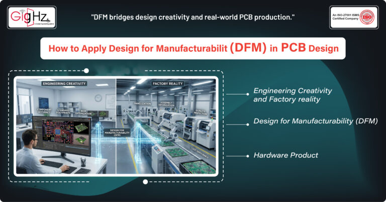
Have you ever spent hours designing a PCB only to discover it can’t be manufactured efficiently?Frustrating, right? You’re not alone.
Many...
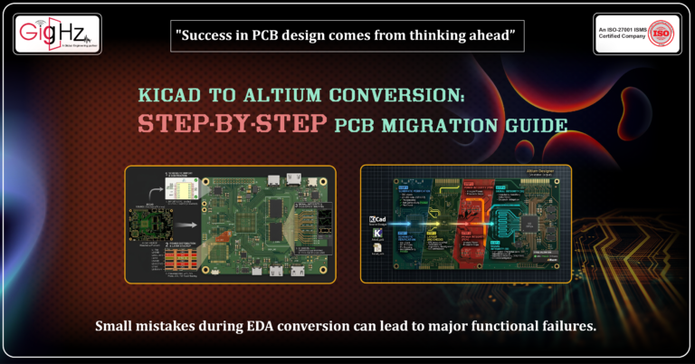
Moving a PCB from KiCad to Altium can seem tricky, especially when working with multi-layer boards. But it doesn’t have to be.
Whether...
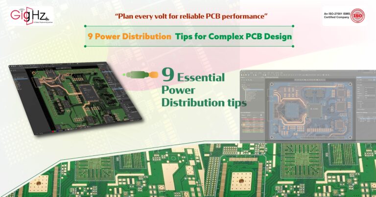
Designing a complex PCB isn’t just about placing components and drawing traces—it’s about ensuring every volt and amp flows exactly...
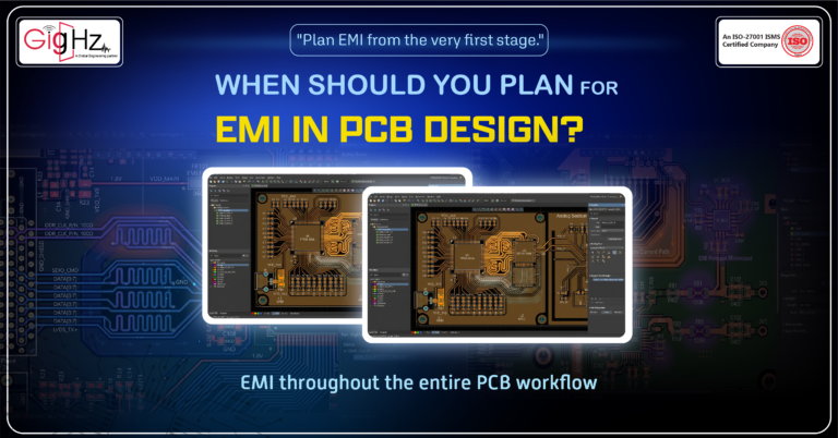
Electromagnetic interference (EMI) is one of the biggest hidden challenges in electronics design.
Many engineers think EMI only matters...
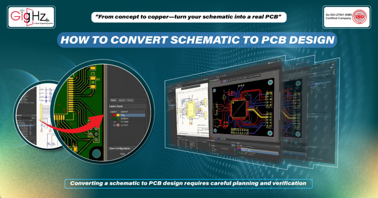
Every electronic product starts with a schematic.
A schematic shows how components connect electrically. It explains how signals move,...
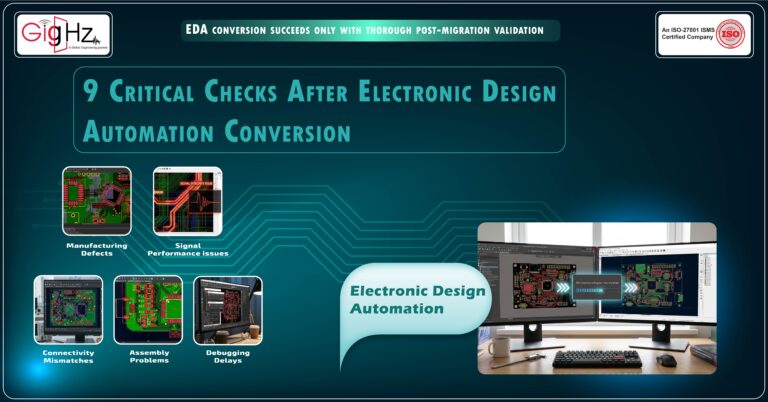
Design conversion is not just about opening a PCB file in another software tool.
In Electronic Design Automation workflows, migration...