

When PCB Space Runs Out, HDI PCB Design Becomes the Answer
- Posted On:
- October 31, 2026
- Category:
- Ecad
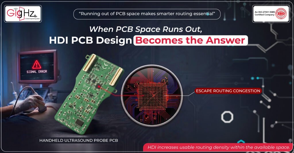
A PCB can have the right components, stackup, and routing plan yet still run out of space. This is common in compact products with fine-pitch BGAs, high pin-count devices, and high-speed interfaces, where escape routing becomes congested and conventional vias or extra layers may increase cost and complexity.
This is where HDI PCB design helps.
HDI does not create more board area; it increases usable routing density within the available space.
What Happens When Conventional Routing Runs Out of Space?
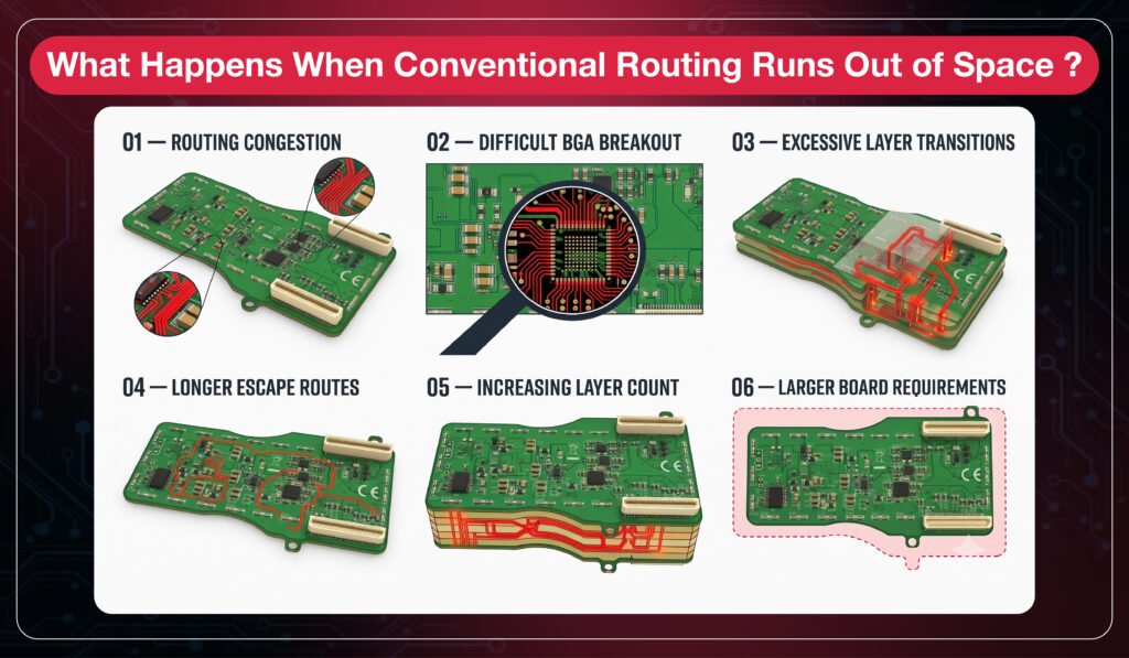
Conventional multilayer boards depend heavily on through-hole vias and standard BGA escape patterns.
As component density increases, these structures consume routing channels and make inner-row BGA connections increasingly difficult.
Typical problems include:
- Routing congestion
- Difficult BGA breakout
- Excessive layer transitions
- Longer escape routes
- Increasing layer count
- Larger board requirements
The real limitation is often the physical space required to connect the signals, not the number of signals alone.
Why Do BGA Packages Create a Routing Bottleneck?
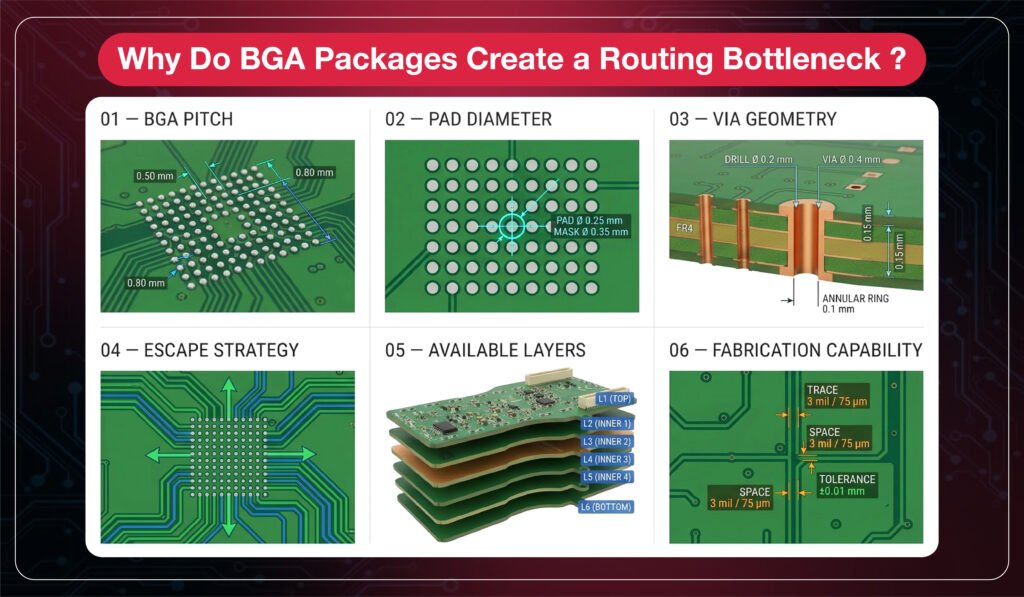
Fine-pitch BGAs are one of the strongest drivers for HDI.
As pitch decreases, the space available between pads becomes smaller. A 0.8 mm-pitch BGA provides considerably less escape space than a 1.0 mm package, while 0.5 mm pitch can make conventional through-hole fanout significantly more restrictive.
The actual requirement depends on:
- BGA pitch
- Pad diameter
- Via geometry
- Escape strategy
- Available layers
- Fabrication capability
A fine-pitch BGA does not automatically require HDI, but 0.8 mm pitch and below can make HDI increasingly attractive in dense designs.
How Does HDI Solve the Space Problem?
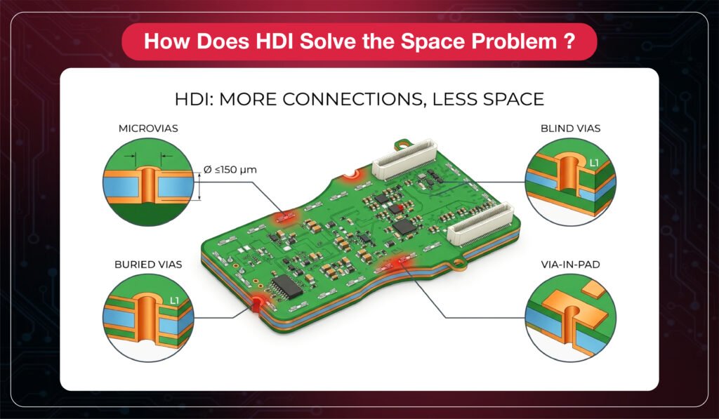
HDI uses smaller, localized interconnect structures to increase routing density.
Microvias
Microvias provide compact layer-to-layer connections. IPC material defines a microvia as a blind hole with a diameter of 150 µm or less.
Blind and Buried Vias
Blind vias connect an outer layer to selected internal layers. Buried vias connect internal layers without consuming outer-layer routing space.
Via-in-Pad
Via-in-pad places the via directly within a component pad, allowing connections to move into internal layers without requiring the same conventional fanout pattern.
The main advantage of HDI is higher interconnect density—not simply smaller vias.
Why Does Microvia Geometry Matter?
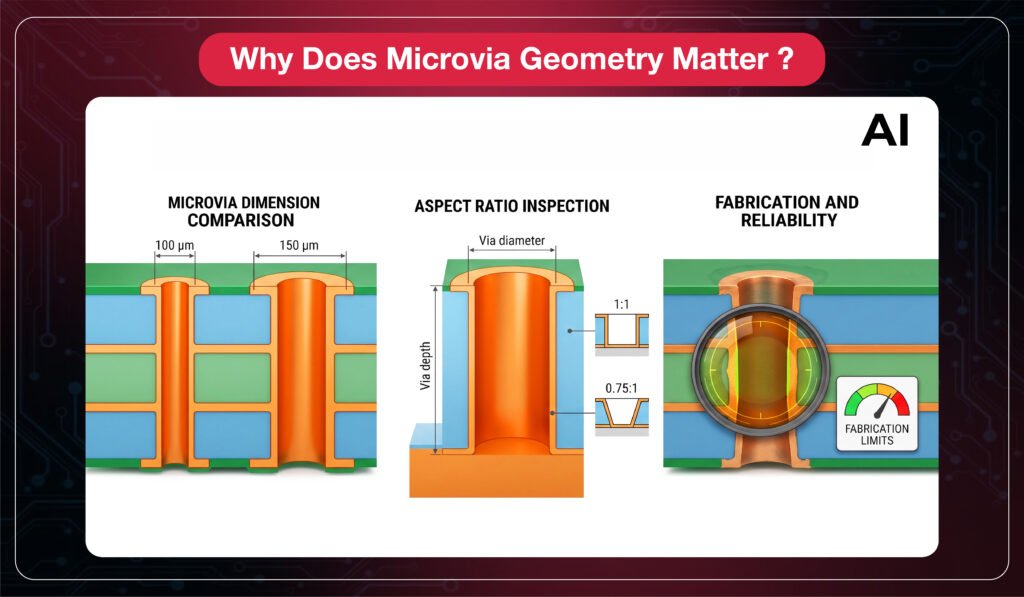
Smaller vias provide routing advantages, but they must remain manufacturable.
Microvia diameters commonly fall around 100–150 µm, although the practical limit depends on the fabricator and board construction.
Aspect ratio is also important. A common HDI design target is around 1:1 depth-to-diameter, while some fabrication processes specify tighter limits such as 0.75:1.
Therefore, engineers should not treat one aspect-ratio value as a universal rule. The final geometry must follow the selected manufacturer’s process capability.
Smaller does not automatically mean better. A microvia must also be reliable and manufacturable.
When Does HDI Actually Make Sense?
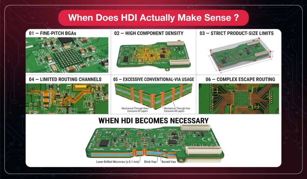
HDI becomes attractive when conventional routing cannot achieve the required connectivity within the available board area.
Consider it when the design has:
- Fine-pitch or high-density BGAs
- High component density
- Strict product-size limits
- Limited routing channels
- Excessive conventional-via usage
- Complex escape-routing requirements
However, HDI is not automatically the better option.
If a conventional multilayer PCB satisfies the electrical, mechanical, reliability, and manufacturing requirements, HDI may introduce unnecessary cost and fabrication complexity.
The right question is not “Can we use HDI?” but
“Do we need HDI to meet the design constraints?”
What Should Engineers Check Before Using HDI?
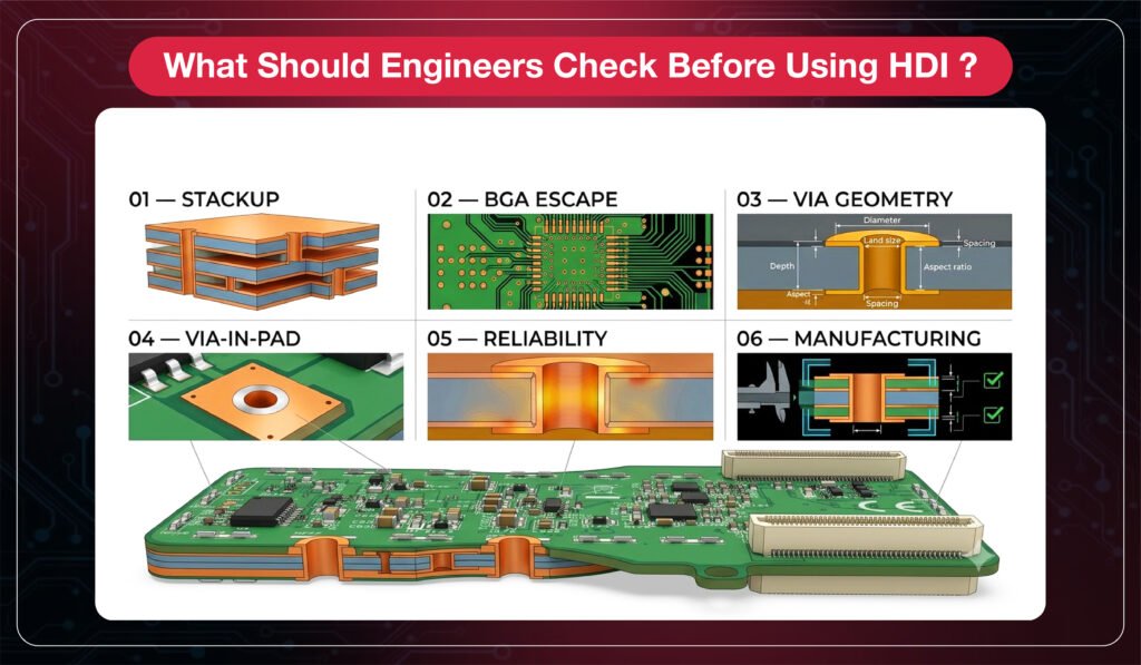
Stackup
Define the build-up structure before routing and identify which layers require microvias.
BGA Escape
Evaluate pitch, pad geometry, via placement, and routing channels before finalizing the escape strategy.
Via Geometry
Check diameter, land size, depth, aspect ratio, spacing, and fabrication limits.
Via-in-Pad
Confirm whether filling and capping are required and account for soldering and reliability requirements.
Reliability
Review microvia plating, thermal cycling, current density, and the reliability implications of stacked structures.
Manufacturing
Confirm the proposed HDI construction with the fabricator before final layout.
What HDI Design Mistakes Cause Rework?
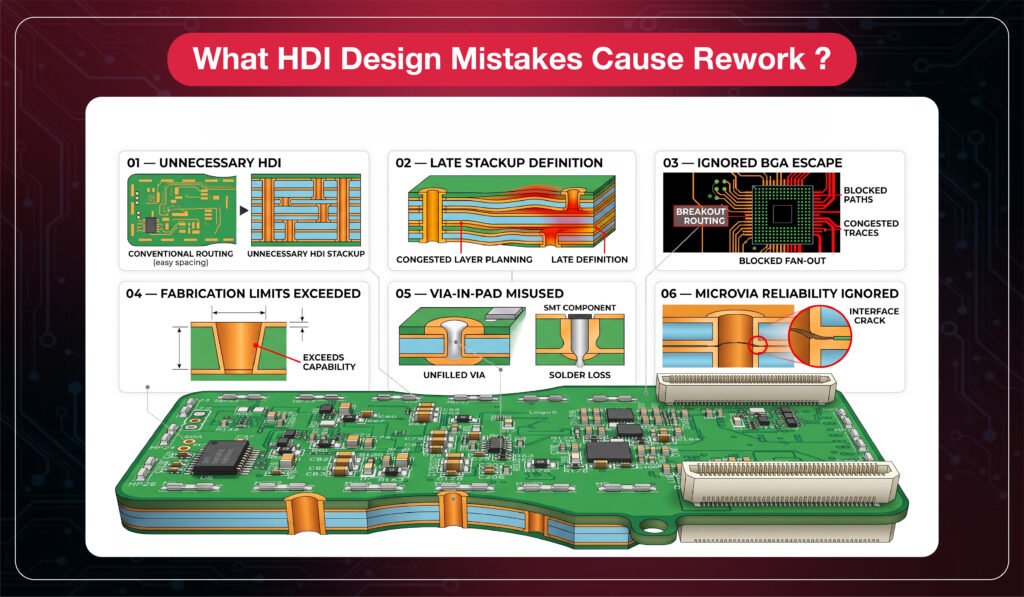
Common mistakes include:
- Choosing HDI without a real density problem
- Defining the stackup too late
- Ignoring BGA escape requirements
- Exceeding fabrication capabilities
- Treating via-in-pad as a simple routing shortcut
- Ignoring microvia reliability
These can lead to redesign, fabrication problems, reliability concerns, and unnecessary cost.
Engineering Insight
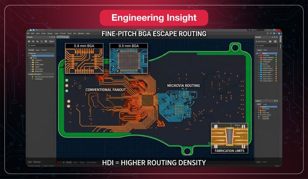
Fine-pitch BGA routing is a common reason engineers consider HDI.
TTM’s guidance shows microvia routing for 0.8 mm BGA devices and below, including a 0.5 mm BGA example. Smaller vias increase localized routing density and provide additional escape paths.
This is useful when conventional fanout consumes too much space or requires extra layers.
However, HDI reliability still depends on via geometry, plating, registration, stacking, and fabrication capability.
HDI’s real advantage is higher routing density—not simply smaller vias.
Final Answer
HDI PCB design becomes the right solution when conventional interconnect structures cannot provide enough routing density within the available board area.
Microvias, blind vias, buried vias, and via-in-pad structures can help engineers escape dense packages and use constrained space more efficiently.
But HDI should not be selected simply because it is more advanced.
The best HDI design solves a genuine density problem while remaining reliable, manufacturable, and cost-effective.
Running out of routing space?
Explore smarter HDI design solutions.
Book a call. Schedule a Free Consultation now. https://calendly.com/gighz/30min
Frequently Asked Questions
- Why can’t I route my BGA with normal vias?
Fine-pitch pads may not leave enough space for conventional fanout. Microvias provide more compact connections. - Why is my PCB getting too large?
Conventional routing may require extra layers or board area. HDI can increase routing density within the same footprint. - Does a 0.5 mm BGA require HDI?
Not always. It depends on the package, stackup, routing space, and fabrication capability. - Is HDI worth the extra cost?
Yes, when conventional routing cannot meet size or density requirements. Otherwise, standard construction may be more economical. - What should I check before choosing HDI?
Review BGA escape, stackup, microvia geometry, via-in-pad, reliability, and fabrication limits.
Stuck in a loop of challenges? Always pick smart solution that works
Have you faced costly rework because 2D drawings skipped in MCAD workflows?
Effective way to prevent MCAD documentation errors recalls?
Please answer both poll questions before submitting.
Thank you for your response! 😊
Latest Post
Get Customized Engineering CAD Design Service

Book a Free Consultation Call
Partner with Gighz and bring your most innovative design concepts to life. Our engineering cad services accelerate development so you can focus on your big vision.
