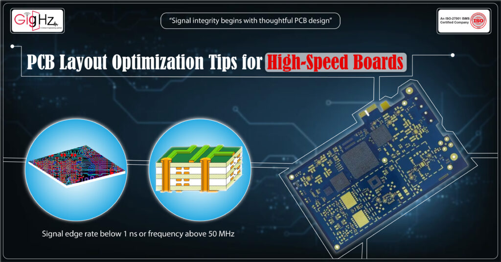
Once the circuits start running at high speeds, even the smallest layout mistake can make a big difference.
Any signal edge rate below 1 ns or frequency above 50 MHz should be treated as high-speed.
Even signals under 100 MHz can behave as transmission lines if trace length exceeds one-tenth of their signal wavelength.
A trace that is only a few millimeters too long, a via placed incorrectly, or a poorly defined ground plane can create serious problems-causing everything from signal distortion to complete communication failure.
That’s why PCB layout optimization isn’t just a design step; it’s a discipline that shapes the performance, reliability, and lifespan of your board.
Whether you’re designing a compact IoT module or a complex networking system, understanding how signals behave at high frequencies is what separates a good PCB from a great one.
In the following blog, we will explain four key areas that every designer should focus on in order to achieve a stable, noise-free, and thermally balanced high-speed PCB layout:
- Signal integrity considerations
- Trace width and routing
- Layer stackup best practices
- Thermal management tips
Let’s dive deeper into each.
1. Signal Integrity Considerations
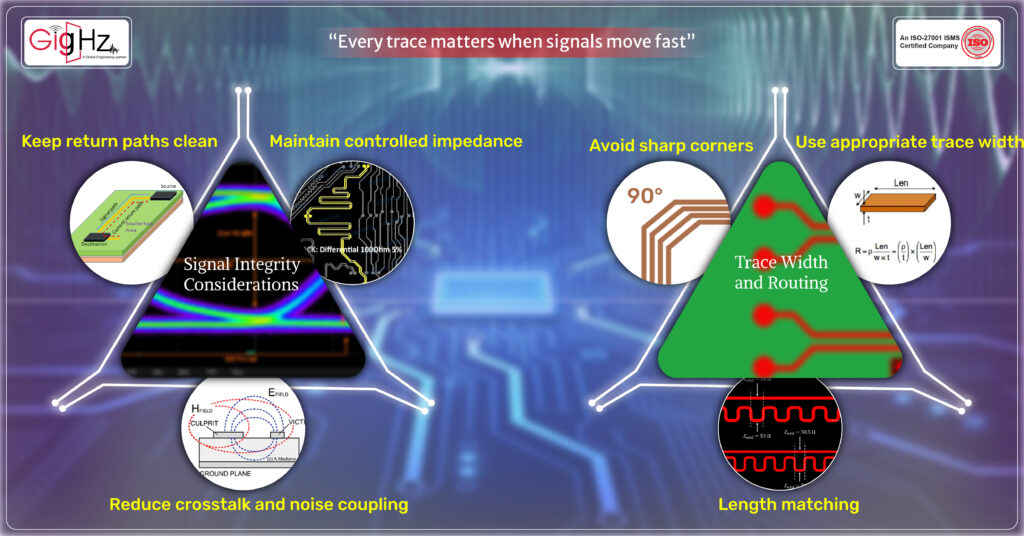
Signal integrity is one of the bases of PCB design for high-speed circuits.
When a signal travels through a trace, it acts more like an electromagnetic wave than a voltage line.
Any impedance variation or reflection causes waveform distortion, timing delay, or affects logic interpretation.
Maintain controlled impedance
For high-speed signals, impedance mismatches cause reflections that corrupt data.
Define controlled impedance lines based on your signal speed and transmission needs.
Typical values vary from 45-60 Ω for single-ended and 85-110 Ω for differential, depending on the interface standards. Correct for many systems: USB, PCIe, HDMI
But not universal. DDR uses ~60 Ω single-ended, 100 Ω differential.
Typical values are from 45–60 Ω single-ended and 85–110 Ω differential, depending on interface standards.
Use your PCB layout optimization software to calculate impedance with high accuracy by taking into consideration dielectric thickness, trace width, and spacing.
The use of field solvers or built-in impedance calculators is common among professional companies to fine-tune this.
Keep return paths clean
Each high-speed signal must have a well-defined return path through the ground plane.
If a trace crosses a split in the reference plane, it forces return current to make a detour; noise is created and crosstalk occurs.
In every layer, there should be continuous ground under the signals.
During routing across layer transitions via, add stitching vias around the signal via to maintain continuity in the return path.
Reduce crosstalk and noise coupling
When two high-speed traces run too close, they start to couple electromagnetically.
This crosstalk can distort data lines and create unpredictable performance.
Keep proper spacing between traces, especially for differential pairs, and avoid parallel routing over long distances.
Keep a spacing of at least 3× the trace width between high-speed single-ended traces to minimize coupling.
Pro Tip: If you must route signals close, add a ground guard trace between them to reduce interference.
2. Trace Width and Routing
The routing of high-speed traces is similar to traffic management on a narrow highway-if one lane is too tight or makes a sharp turn, the signals slow down or collide.
Optimized routing allows the signals to travel smoothly with minimum distortion and delay.
Use appropriate trace width
Trace width isn’t just about fitting components; it is directly related to resistance, inductance, and impedance.
Wider traces lower the resistance and heat but can change impedance values.
The ideal trace width depends on your stackup and dielectric material.
Use impedance calculators as part of the PCB layout optimization process to define exact widths for critical nets, such as DDR data lines, clocks, or differential pairs.
Avoid sharp corners
90-degree corners serve as tiny capacitors, reflecting the signals and causing EMI.
High-speed traces must always use either 45-degree bends or rounded corners. It improves the flow of signals, as well as manufacturability.
Length matching
Timing is everything in differential signals or parallel data buses. Even 1mm of trace length difference can cause skew that breaks synchronization.
Match trace lengths carefully for all high-speed signals, especially the DDR, USB, and Ethernet lines.
Pro Tip: In high-speed design, routing should not only be about connection — it’s about timing control.
3. Layer Stackup Best Practices
Your PCB layer stackup defines the way signals travel, return, and interact across layers.
For high-speed circuits, the stackup defines impedance control, EMI performance, and overall board reliability.
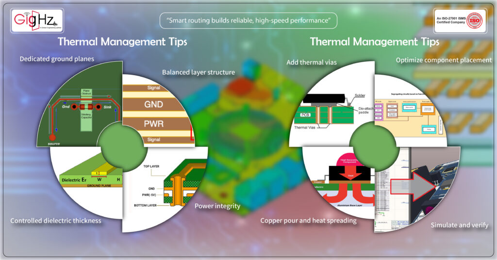
Balanced layer structure
Use a symmetrical stackup such as signal–ground–power–signal or signal–ground–signal–power.
The symmetry ensures predictable impedance and minimizes warping during fabrication.
Dedicated ground planes
A continuous ground plane beneath the signal layers provides shielding and a reference return path.
It reduces EMI, stabilizes impedance, and improves signal quality. Never compromise your ground layer to save space — it’s the most valuable layer in high-speed design.
Controlled dielectric thickness
Dielectric thickness between the signal and ground layer impacts impedance and propagation delay, so it should be uniform and according to your controlled impedance requirements.
Most Professional PCB design companies use standard prepregs and cores to achieve tight dielectric tolerances for consistent high-speed behavior.
Power integrity
Power planes should be closely coupled to ground planes to provide low-inductance decoupling.
This is very important as voltage fluctuations and noise may become worse in the high-frequency range.
Always position decoupling capacitors close to power pins of ICs.
Pro Tip: Decide your stackup before any routing begins. Changing it in the middle will break impedance control and timing budgets.
4. Thermal Management Tips
With the increase in the signal speed, the generation of heat also increases.
High-speed boards often carry dense components, switching regulators, and fast transceivers that generate localized hotspots.
Ignoring thermal design can cause premature failure or signal drift.
Optimize component placement
Place high-power components, such as regulators and processors, away from sensitive analog or RF areas. Ensure there’s enough airflow around the heat-generating parts.
Add thermal vias
Arrays of thermal vias beneath power devices or ground pads transfer heat efficiently to inner or opposite layers.
The simple yet powerful PCB layout optimization trick reduces surface temperatures dramatically.
Copper pour and heat spreading
Use large copper areas or ground fills to distribute the heat evenly. Copper is a natural heatsink, especially if interconnected through multiple vias.
Just ensure these copper pours don’t interfere with signal impedance or routing paths.
Simulate and verify
Many of today’s PCB design services include thermal simulation at layout.
Tools such as Altium, Cadence, or Ansys Icepak help you identify hot zones before manufacturing.
This proactive approach can save both cost and performance headaches later.
Bottom Line
High-speed PCB design is not about faster signals, but about control, balance, and foresight. Every trace, via, and layer decision you make creates a measurable difference in performance.
By focusing on signal integrity, trace routing, layer stackup, and thermal management, you will create designs that work well on paper but also perform perfectly in real-world applications.
For next-level PCB layout optimization, it helps to work with a professional PCB design company with a deep understanding of the physics behind every signal path.
From impedance tuning to thermal simulation, their PCB Design Services will ensure that the board performs reliably under demanding conditions.
In high-speed design, perfection isn’t optional-it’s a necessity. Start your next project with precision, and your board will thank you through performance that never skips a beat.
Book a Call. Schedule a Free Consultation now https://calendly.com/gighz/30min
Stuck in a loop of challenges? Always pick smart solution that works
Have you faced costly rework because 2D drawings skipped in MCAD workflows?
Effective way to prevent MCAD documentation errors recalls?
Please answer both poll questions before submitting.
Thank you for your response! 😊
Latest Post
Get Customized Engineering CAD Design Service

Book a Free Consultation Call
Partner with Gighz and bring your most innovative design concepts to life. Our engineering cad services accelerate development so you can focus on your big vision.