Essential DFM Checks Every University Project Management Should Include
- Posted On:
- January 6, 2026
- Category:
- Ecad
Every university PCB project starts with a working prototype — the LEDs blink, power flows, and the board performs as expected.
But once it’s sent for fabrication, problems start to appear:
trace width below limit, via size too small, silkscreen on pads.
These are not design bugs — they are manufacturability issues.
They occur because the layout was optimized for function, not for production.
That’s where Design for Manufacturability (DFM) becomes essential.
DFM means designing a PCB in a way that can be easily and accurately manufactured by the fabrication process.
It’s a technical practice that ensures your PCB can be fabricated, assembled, and tested within real manufacturing constraints.
It helps designers align their layout with fabrication rules — controlling trace widths, clearances, hole sizes, and material limits — to prevent redesigns and production delays.
For university teams and early-stage startups, applying DFM early builds the habit of designing boards that are not just functional but also ready for scalable manufacturing.
The Hidden Layer of Manufacturing Readiness
Most student projects stop at functionality.
They consider the design functionally validated when the circuit passes simulation or when a prototype runs on a breadboard.
But manufacturing brings a new set of physical realities — copper width, hole size, spacing, heat, and mechanical alignment.
These are things that software simulations don’t complain about, but a PCB manufacturer definitely will.
That’s why project management in universities should treat DFM checks as part of the design process, not as an afterthought.
Trace Width and Spacing — The Foundation of Reliability
Every trace on your PCB does more than just carry current — it defines how reliable and manufacturable your board will be.
If a trace is too narrow for the expected current, it can overheat, cause voltage drop, or even burn open.
If two traces are placed too close, the risk of short circuits, solder bridging, or dielectric breakdown increases during fabrication and operation.
Trace width determines how much current a conductor can safely carry without excessive temperature rise, while spacing ensures proper electrical isolation between signals and prevents arcing or crosstalk.
For example, if your manufacturer specifies a minimum of 6 mil trace width and 6 mil spacing, but your design uses 4 mil, it becomes a fabrication violation — meaning the traces might not etch correctly, or they could fail under load.
Even a 2-mil deviation can compromise both electrical reliability and yield.
That’s why a proper Design Rule Check (DRC) must always be performed using parameters aligned with your manufacturer’s capability.
It’s a simple check that ensures your design doesn’t just work electrically — it can actually be produced with consistent quality and reliability.
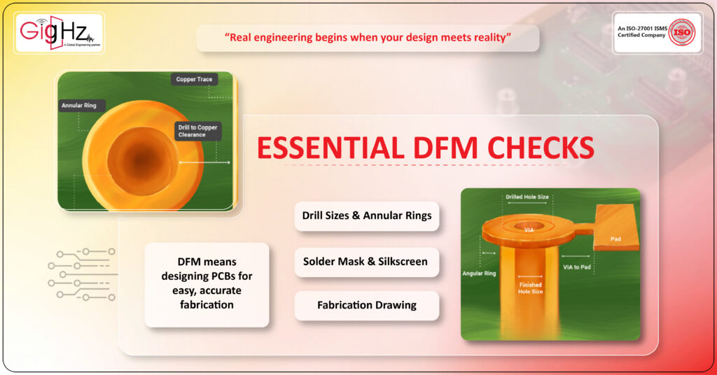
1. Drill Sizes and Annular Rings — Where Precision Meets Production
In PCB design software, vias and holes may look simple — just circles on different layers.
But in real fabrication, they define mechanical strength, layer alignment, and electrical continuity across the board.
Each via consists of a drilled hole and a surrounding annular ring — the copper pad area that ensures electrical connection between layers after plating.
If the drill size is too small compared to the board thickness, it increases the aspect ratio (board thickness ÷ hole diameter), making plating inside the hole difficult and potentially causing voids or open vias.
If the drill bit tolerance isn’t matched with the minimum annular ring width, even slight drill misregistration can cause the hole to break out of the pad — leaving insufficient copper around the barrel.
Similarly, if the annular ring is too thin, the copper plating may not adhere evenly, leading to weak joints or intermittent connections between layers.
Even a single missing or incomplete ring can interrupt an entire signal path, especially on high-density or multilayer PCBs.
That’s why every design should include a DFM check for minimum drill size, annular ring width, drill-to-copper clearance, and aspect ratio — all aligned with the manufacturer’s fabrication limits.
Precision in these dimensions directly translates to better yield, stronger interconnections, and higher long-term reliability.
2. Component Placement — The Art of Physical Thinking
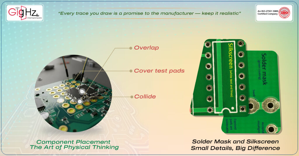
In a university lab, components often fit perfectly on the layout screen.
But during assembly, they might collide, overlap, or even cover test pads.
Real boards are three-dimensional.
Capacitors, connectors, and heat sinks have volume.
Without proper spacing, rework becomes painful and soldering becomes inconsistent.
That’s why every project manager should make 3D placement checks a rule.
It’s not just about looking neat — it’s about ensuring your board can be assembled and reworked safely.
3. Solder Mask and Silkscreen — Small Details, Big Difference
A minor misalignment in solder mask openings can lead to solder bridges.
A silkscreen text printed on a pad may burn off during soldering.
These may sound like small errors, but they cost real time and money in fabrication.
When you validate your DFM, ensure that solder mask openings match pad positions and silkscreen markings stay clear of copper.
This simple discipline turns a student board into a professional-grade product.
4. Thermal Relief and Copper Balance — The Science of Heat and Stability
Thermal management isn’t only for high-power boards — even simple university projects can suffer from poor heat flow.
When a large copper plane connects directly to a pad, soldering that pad becomes difficult because heat spreads away too quickly.
That’s why thermal relief patterns are added — they help maintain consistent solder joints.
At the same time, uneven copper distribution can cause warpage during lamination.
When one layer has heavy copper and another is sparse, the board bends slightly — enough to affect assembly.
Including copper balance and thermal relief checks in your DFM process ensures both reliability and manufacturability.
5. Test Points — Because Debugging Is Part of Design
Testing is not an optional step; it’s part of every design’s lifecycle.
Adding accessible test points makes life easier for both engineers and manufacturers.
Without them, probing power lines or signal paths during testing becomes messy and error-prone.
A good DFM mindset ensures that test pads are placed logically, easily reachable, and clearly marked.
This small habit separates a “student project” from a “real product.”
6. Fabrication Drawing and Layer Stack — The Blueprint for Production
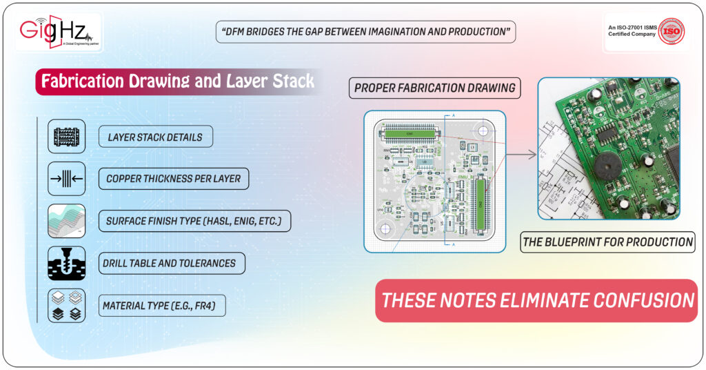
Imagine sending your design files to a manufacturer without mentioning copper thickness or layer order.
It’s like sending a map without directions.
A proper fabrication drawing is your communication bridge with the production floor.
It should include:
- Layer stack details
- Copper thickness per layer
- Surface finish type (HASL, ENIG, etc.)
- Drill table and tolerances
- Material type (e.g., FR4)
These notes eliminate confusion and help fabricators reproduce exactly what you designed.
The Real Value of DFM in University Projects
University projects aren’t just about grades — they’re training grounds for future engineers.
When students learn DFM early, they understand how design choices affect cost, yield, and quality.
For startups emerging from universities, this understanding becomes a competitive advantage.
You won’t just design something that “works”; you’ll design something that “can be built” — consistently and affordably.
A project that passes DFM checks once is a project that’s ready for the real world.
Bottom Line
Designing a PCB that works is good.
Designing one that can be manufactured without errors — that’s great engineering.
That’s what DFM really teaches: to think beyond software, beyond theory, and into reality.
Every trace, every pad, every layer carries a physical truth.
Ignoring those truths leads to fabrication failures and wasted effort.
But respecting them — through Design for Manufacturability (DFM)— builds a culture of precision, responsibility, and engineering maturity.
So as your next university project takes shape, don’t stop at design completion.
Ask yourself one final question before calling it “done”.
Book a Call. Schedule a Free Consultation now https://calendly.com/gighz/30min
Stuck in a loop of challenges? Always pick smart solution that works
Have you faced costly rework because 2D drawings skipped in MCAD workflows?
Effective way to prevent MCAD documentation errors recalls?
Please answer both poll questions before submitting.
Thank you for your response! 😊
Latest Post
Get Customized Engineering CAD Design Service

Book a Free Consultation Call
Partner with Gighz and bring your most innovative design concepts to life. Our engineering cad services accelerate development so you can focus on your big vision.