When you finally finish your PCB layout, it feels like a huge milestone.
Every component is placed, every trace is routed, and you’re ready to send it for fabrication.
But then, the manufacturer replies with something you don’t expect —
“We found issues in your design.”
It’s a message that instantly stalls everything.
Production gets delayed, your schedule shifts, and your excitement fades into frustration.
The worst part?
These delays usually don’t come from complex electrical problems.
They come from small design decisions — things that seemed fine during layout but didn’t meet real-world manufacturing limits.
PCB design and manufacturing are deeply connected.
When the design doesn’t align with fabrication, assembly, and testing capabilities, time is lost in rework, communication, and sometimes, full redesigns.
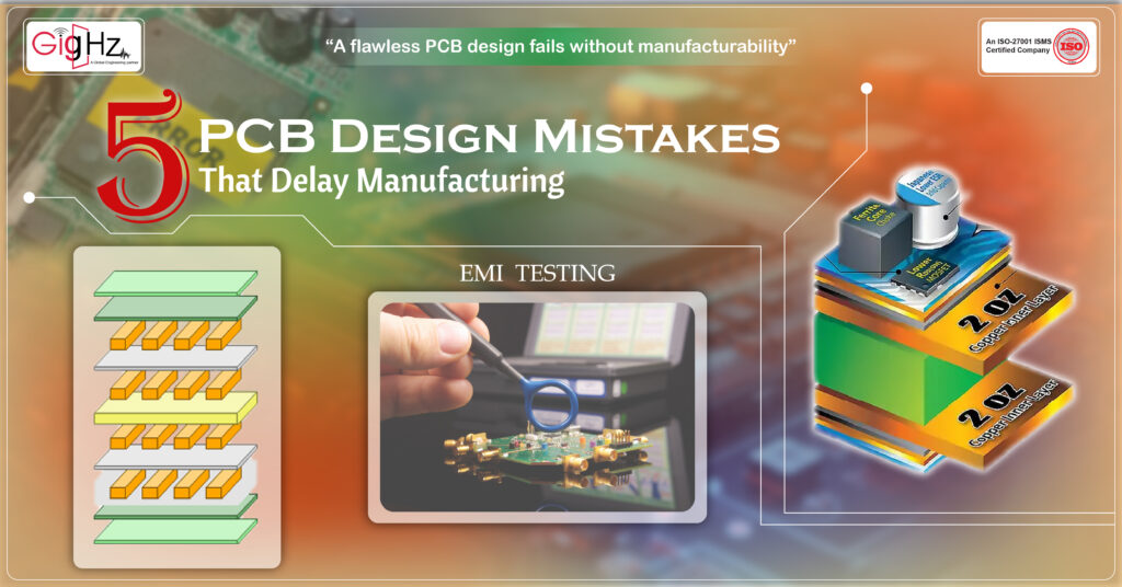
Let’s go through five common PCB Design mistakes that quietly cause these delays — and understand what really happens behind them.
Ignoring DFM Guidelines
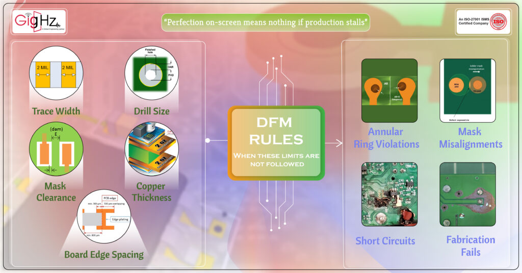
The first and most common mistake happens before manufacturing even starts — ignoring Design for Manufacturability (DFM) guidelines.
DFM defines the limits of what your PCB fabricator can produce, like minimum trace width, drill size, solder mask clearance, copper thickness, and board edge spacing.
When these limits are not followed, fabrication either fails or pauses for clarification.
For example, imagine routing your signals with 4 mil traces, but your fabricator only supports 6 mil. Or placing vias too close to copper pours, which can break during drilling.
These seem minor, but they lead to annular ring violations, mask misalignments, and even short circuits during assembly.
The reason this causes delay is because manufacturers can’t fix it themselves.
They’ll send back the file asking for a revision, and you’ll lose days correcting something that could have been avoided.
That’s why the best approach is to start your design with DFM rules in place.
Most ECAD tools, like Altium Designer, KiCad, or OrCAD, allow you to import DFM constraints directly.
When you route within those limits, your design will move through fabrication without interruption.
Poor Component Placement
Once DFM is under control, the next problem often shows up in the layout stage — poor component placement. Avoid placing components within 100 mils of board edge.
A PCB might look neat on-screen, but poor placement can make assembly complicated and even affect board performance.
If polarized components face different directions, pick-and-place machines slow down. If tall components are placed near connectors, they can block access.
And if power parts are clustered too close, heat buildup can cause long-term reliability issues.
Technically, placement affects signal flow, thermal management, and assembly orientation.
A simple example: placing a voltage regulator too far from its load increases trace resistance and voltage drop.
Similarly, putting analog and digital ICs close together without isolation introduces noise.
The ideal approach is to divide your board into functional zones — power section, signal section, and control section.
Keep decoupling capacitors close to IC pins, align polarized parts consistently, and leave enough spacing for soldering tools and inspection.
A board that’s laid out logically doesn’t just look better — it moves through assembly faster and has fewer rework chances.
Inadequate Routing & Trace Widths
Routing is where design becomes reality. Every trace you draw defines how current and signals move through your board.
But when traces are undersized or poorly routed, it leads to serious problems in manufacturing and testing.
If a trace carrying high current is too narrow, it heats up under load. For example, a 1 oz copper layer can safely carry about 1A current through a 25 mil wide trace.
Anything thinner risks voltage drop, overheating, or even burning during operation.
On the signal side, improper routing causes impedance mismatch and crosstalk. Unequal differential pair lengths or unbalanced return paths can distort signals.
These are not visible in your CAD design but appear during high-speed testing or functional validation.
Return path is equally critical. Every signal current needs a clear and continuous return path beneath its trace, usually through the ground plane.
If the return path is broken by splits, gaps, or via transitions, the current is forced to find alternate routes — creating loops that increase inductance and noise.
This can severely degrade signal integrity, especially in high-speed designs.
Always ensure that ground planes remain solid and uninterrupted under signal traces, and provide stitching vias wherever signals cross plane boundaries.
To prevent this, always calculate trace widths based on current and copper thickness using tools like the IPC-2221 calculator.
Keep high-speed traces short, parallel differential pairs matched, and avoid unnecessary vias that add inductance.
Routing isn’t just about completing connections — it’s about maintaining controlled current flow, consistent impedance, and reliable signal paths throughout your design.
Not Considering Signal Integrity & EMI
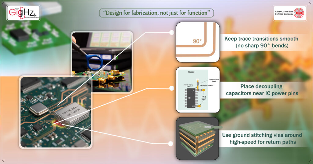
One of the most underestimated areas in PCB design is Signal Integrity (SI) and Electromagnetic Interference (EMI).
Designers often focus on completing connections but forget that every trace also acts as an antenna.
When traces are long, unshielded, or routed over split planes, they can reflect signals, radiate energy, and interfere with nearby lines.
These issues often don’t appear until EMI testing, which happens after fabrication — meaning if the board fails, you’re back to redesigning.
For example, high-speed differential signals should be routed together with consistent spacing and controlled impedance.
If their lengths vary or cross plane splits, they lose synchronization.
Similarly, power traces that run parallel to sensitive analog lines can inject switching noise.
To avoid this, maintain a solid ground plane, keep trace transitions smooth (no sharp 90° bends), and place decoupling capacitors near IC power pins.
Use ground stitching vias around high-speed or noisy areas to create return paths and minimize radiation.
By designing with signal integrity in mind, your board passes testing faster, and you avoid the costly cycle of redesign and revalidation.
Overlooking Testing & Verification
Finally, one of the biggest time-wasting mistakes happens right before you send files for production — skipping testing and design verification.
It’s easy to assume your schematic and layout are correct, but even small errors can cause major delays later.
Missing test points, incorrect footprints, or swapped pins are among the most common reasons for rework.
Before finalizing, every board should go through a complete ERC (Electrical Rule Check) and DRC (Design Rule Check).
These automated checks help catch open nets, clearance issues, and incorrect pad spacing.
But manual reviews are just as important — comparing footprints against datasheets, verifying connector orientations, and ensuring all critical signals have accessible test points.
Test points are not just for debugging. They make in-circuit testing (ICT) and functional verification faster during manufacturing.
A board with clear access to major signals reduces test time and avoids manual probing during production.
Design verification might feel like the last step, but it actually ensures the first-pass success of your entire manufacturing process.
Bottom Line
Every PCB delay has a root cause — and in most cases, it starts with the design.
When you ignore DFM limits, place components without logic, route traces carelessly, skip EMI control, or overlook testing, you create invisible barriers that only show up during production.
The goal of a PCB designer is not just to make the circuit work — it’s to make it manufacturable, testable, and reliable from the very first batch.
By aligning design rules with manufacturing capabilities, verifying every footprint, controlling trace geometry, and considering signal behavior early, you build a design that moves smoothly through fabrication and assembly — without the back-and-forth delays that waste both time and cost.
Because in PCB design mistakes, success isn’t when the layout looks perfect on your screen — it’s when your board reaches production, passes testing, and performs exactly as designed, the very first time.
Book a Call. Schedule a Free Consultation now https://calendly.com/gighz/30min
Stuck in a loop of challenges? Always pick smart solution that works
Have you faced costly rework because 2D drawings skipped in MCAD workflows?
Effective way to prevent MCAD documentation errors recalls?
Please answer both poll questions before submitting.
Thank you for your response! 😊
Latest Post
Get Customized Engineering CAD Design Service

Book a Free Consultation Call
Partner with Gighz and bring your most innovative design concepts to life. Our engineering cad services accelerate development so you can focus on your big vision.