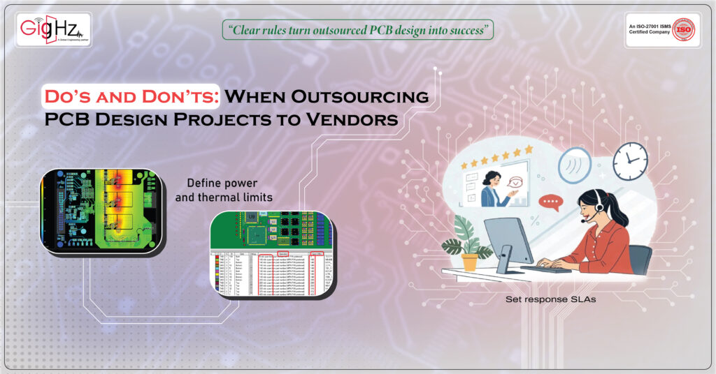
Ecad

PCB EMC design errors

Top 5 PCB Layout Mistakes That Cause Radiated Emissions in High-Speed Designs

So, you must have optimised the schematic, chosen the right components, and even double-checked stack-up rules. But when the board hits EMI testing, it fails. Now, this is often the result of subtle PCB layout mistakes causing radiated emissions—issues that don’t show up in design reviews but quickly surface in the compliance lab. In high-speed

Top 5 PCB Layout Mistakes That Cause Radiated Emissions in High-Speed Designs Read More »

Why PDN Design Fails on Real PCB Despite Passing Simulation

So, apparently, you must have run all the simulations, where everything looks stable, and the margins seem completely  safe. But when the board comes back from fabrication, the measurements don’t match the models. This kind of PDN design failure after simulation is one of the most common and frustrating issues engineers face. Now, on paper,

Why PDN Design Fails on Real PCB Despite Passing Simulation Read More »

PCB cost vs reliability

How to Preserve Netlist & BOM Accuracy During EDA Migration

As we all know, it goes without saying that switching ECAD platforms is never as simple as clicking “export” and “import.” Yes, If you’ve ever tried migrating a project from one tool to another, you are well familiar with the risk of data slipping through the cracks. On the other hand, symbols lose pin mappings,

How to Preserve Netlist & BOM Accuracy During EDA Migration Read More »

footprint mismatch in PCB layout

Why Your PCB Layout Doesn’t Match the Schematic — and How to Fix It

So, you have double-checked your design, right? Likewise, the schematic is clean, ERC passed, and you are feeling confident. But when you push the design to layout, the problem hits significant: As a result nothing fits. Now, this dreaded PCB layout doesn’t match schematic problem and it’s apparently more common than you think. Engineers worldwide

Why Your PCB Layout Doesn’t Match the Schematic — and How to Fix It Read More »

pcb design fail

Why Most PCB Designs Fail in First Manufacturing and How to Prevent

Nearly 70% of new PCB designs fail in their very first manufacturing run. Yes, engineers invest weeks of effort into schematics and layouts but only to watch the first prototypes come back with issues like: Short circuits Open enclosures  Assembly issues, or signal problems And while people often blame complexity or tight deadlines, the real

Why Most PCB Designs Fail in First Manufacturing and How to Prevent Read More »

first time pass design

Is First-Time Pass PCB Design Possible? Here’s What You Need to Know

Truly, every engineer dreams of having a First-Time Pass PCB Design process!  Accordingly, sending a board for fabrication, then getting it assembled, and seeing it work flawlessly on the first go. Moreover, No re-spins, no unexpected failures and of course no budget overruns. But is that even realistic, or just wishful thinking? Well, the truth

Is First-Time Pass PCB Design Possible? Here’s What You Need to Know Read More »

How to Avoid Crosstalk at 16GHz in High-Speed Automotive PCB Design

Undoubtedly, at 16 GHz, even the tiniest layout oversight can turn into a full-blown performance disaster. That’s why we learned this the hard way on a recent EV controller project, where crosstalk in PCB design almost derailed our timing margins completely. That too…just a few days before prototype release. Likewise, in high-speed automotive boards, crosstalk

How to Avoid Crosstalk at 16GHz in High-Speed Automotive PCB Design Read More »

How We Cut BOM by 18% in an EV Project—Without Losing Features

“18% BOM cost down, zero functionality loss, no redesign delays.” When we first got the call, the client was already behind the schedule! Yes, it truly happened.  Evidently, their entire EV platform was entering design validation, and the bill of materials was becoming gigantic day-by-day which was beyond the original cost targets. So, they asked

How We Cut BOM by 18% in an EV Project—Without Losing Features Read More »

How to Avoid PCB Design Mistakes Before Manufacturing

Finishing a PCB design always feels good. You see the layout on your screen, and everything seems in place. But the real challenge begins once the board is manufactured. That’s often when hidden mistakes show up—sometimes small, but costly enough to cause failure. The tricky part is that most problems don’t come from advanced engineering

How to Avoid PCB Design Mistakes Before Manufacturing Read More »

Scroll to Top