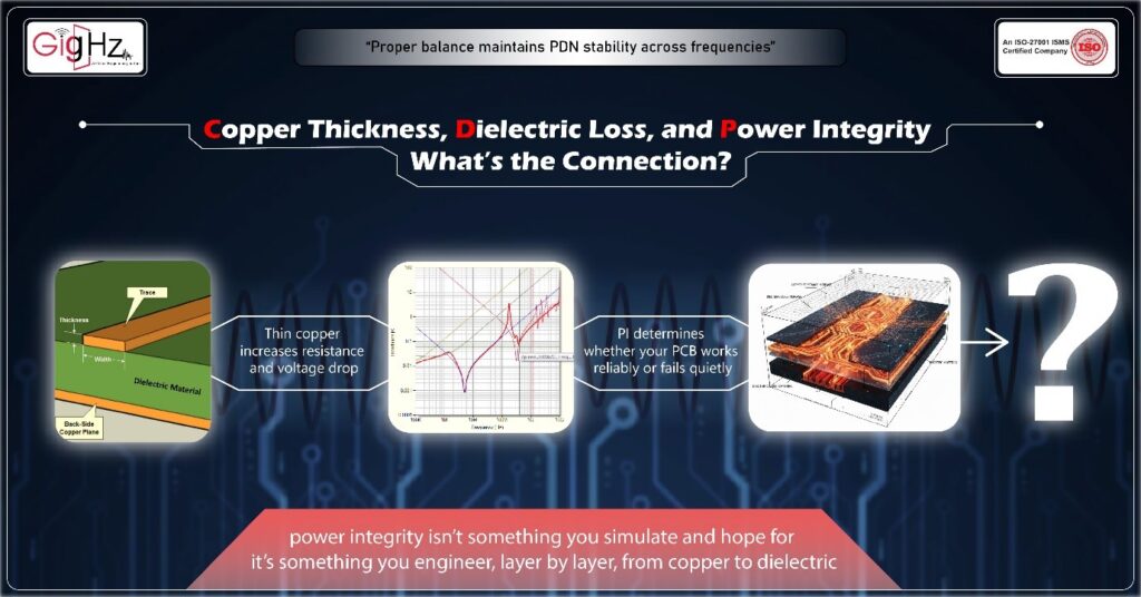
Copper Thickness, Dielectric Loss, and Power Integrity What’s the Connection?
- Posted On:
- December 3, 2025
- Category:
- Analysis & Simulation
Every PCB designer has faced that frustrating moment: the simulation looks flawless, but the real board doesn’t behave as expected.
Maybe the voltage dips under load, noise creeps into sensitive circuits, or thermal hotspots appear out of nowhere.
Often, the root cause isn’t obvious. It’s hidden in the materials themselves — the copper that carries your power, and the dielectric that insulates it.
These two factors, combined with the design of your power network, define power integrity, which determines whether your PCB works reliably or fails quietly.
In this blog, we’ll explore copper thickness, dielectric loss, and power integrity — why they matter, how they are connected, and how small material choices can ripple into big electrical consequences.
By the end, you’ll understand how to engineer a PCB where power integrity is built into the foundation, not just simulated on a screen.
Copper Thickness – The Pathway of Power
Copper thickness is often the first parameter you define when building a PCB stack-up. It decides how much current each trace or plane can safely carry.
The thicker the copper, the lower the resistance. Lower resistance means less voltage drop, less heat, and more stable power delivery.
But that’s only the beginning.
When copper is too thin, the resistance increases. You might not notice it in low-current signals, but for power planes, it can cause significant IR drop — the voltage drop that occurs as current flows through resistance.
Even a small loss here can make your ICs run out of their voltage tolerance window.
For example, if your design expects 1.0V at the processor pin and loses 30mV on the way due to copper resistance, that’s already a 3% loss.
Under heavy load, that drop increases, and suddenly the system becomes unstable.
On the other hand, thicker copper isn’t always a perfect solution.
It adds cost, makes fine routing harder, and changes the impedance of power and signal lines.
The thicker the copper, the lower the characteristic impedance — and if this isn’t managed properly, it can affect return paths and cause signal reflections.
So, copper thickness is not just about carrying current. It’s about maintaining a predictable, uniform electrical path that ensures your power integrity stays intact.
Dielectric Loss – The Invisible Energy Drain
Now let’s look at the layer between copper — the dielectric. It’s meant to insulate, but it also interacts with electromagnetic fields as current and signals travel across your board.
Every dielectric material, from FR4 to high-performance laminates, has two key properties: dielectric constant (Dk) and dissipation factor (Df).
The Dk defines how fast signals travel. The Df — or dielectric loss — defines how much energy gets lost as heat while signals and power flow.
Here’s where it connects to power integrity:
When dielectric loss is high, part of your energy literally disappears as heat.
That loss doesn’t just affect high-speed signals — it also impacts power plane stability.
The distributed capacitance between power and ground planes relies on dielectric properties.
If that dielectric is loss, it weakens your ability to smooth voltage fluctuations across the board.
In simpler terms, the dielectric decides how “clean” and “efficient” your power planes are.
A lossy dielectric turns some of your power into heat, causes phase shifts, and increases ripple and noise in the power network.
You may not see dielectric loss directly on a scope, but you’ll sense its effect — in higher temperatures, unstable power rails, or unexplained EMI problems.
It’s like a silent drain, constantly stealing a fraction of your power integrity.
How They Work Together – The Real Connection
Now comes the interesting part — how copper thickness and dielectric loss connect to define power integrity.
Think of your power distribution network (PDN) like a system of pipes.
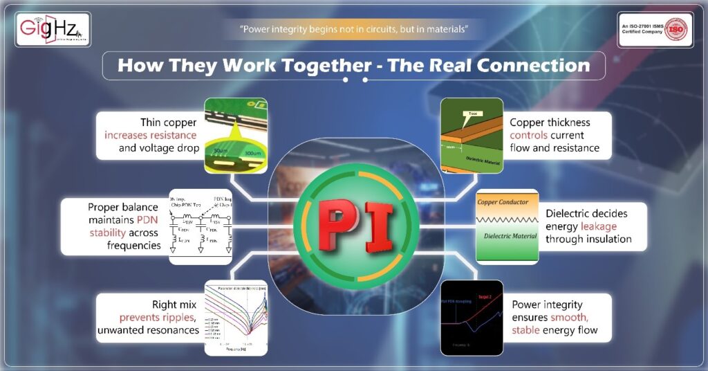
- The copper thickness defines how wide the pipes are — how freely the current can move.
- The dielectric defines how much energy leaks through the energy dissipation.
- Power integrity is the stable and low impedance delivery of power across the PDN.
If the copper is too thin, you face resistance is high and voltage drop.
If the dielectric is too lossy, energy leaks as heat or noise.
Together, they decide how low your PDN impedance can be and how well your board responds to fast load changes.
Power integrity depends heavily on impedance matching across frequencies.
Copper resistance dominates at low frequencies, while dielectric loss dominates at high frequencies.
The right combination ensures that your PDN remains stable from DC to MHz ranges, avoiding unwanted resonances and voltage ripples.
In short, copper thickness and dielectric loss are two ends of the same bridge — one conducts, the other insulates — but both determine how your power really behaves under load.
When the Balance Breaks
Let’s say you use thin copper to save cost, and pair it with a standard FR4 dielectric.
At low current, it might look fine. But under higher load, the voltage starts to decrease. The return current paths heat up.
The dielectric warms too, and its loss tangent increases, creating even more loss. Before long, your PDN impedance spikes, and power noise reaches your IC pins.
You might notice clock jitter, random resets, or EMI issues — all of which trace back to material-level imbalance.
The result? You redesign the board, thinking it’s a layout issue.
But the real problem was the material stack-up that didn’t support the electrical demand.
In high-speed or high-current designs, even small mismatches in copper thickness or dielectric properties can trigger costly redesigns.
Power integrity doesn’t fail suddenly — it fades gradually, as resistance and loss eat away your voltage stability.
That’s why experienced designers always check the physical limits of their materials, not just the electrical models.
How to Get the Balance Right
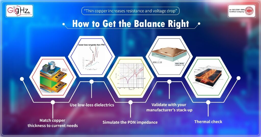
The key is to balance conductivity and insulation — not maximize one at the expense of the other.
Here’s how you can do it right:
- Match copper thickness to current needs. Use design tools to calculate voltage drop and temperature rise. For heavy current planes, 2 oz copper may be worth the extra cost.
- Use low-loss dielectrics if your board carries high-speed signals or sensitive power rails. Materials like Rogers or Isola have lower loss tangents than FR4.
- Simulate the PDN impedance with accurate material parameters. Include both copper resistance and dielectric loss in your model.
- Validate with your manufacturer’s stack-up. Real copper plating thickness and dielectric constants often differ from nominal values.
- Thermal check: As temperature rises, copper resistance and dielectric loss both increase — so thermal simulation helps predict behavior in real conditions.
The right balance ensures your PDN delivers steady power without unnecessary heat or noise.
Bottom Line
Power integrity isn’t just an electrical problem — it’s a material story. Every electron moving across your board depends on copper that can carry it efficiently, and dielectric that can insulate it without draining energy.
Neglecting copper thickness or dielectric properties may seem minor in the design phase, but in the real world, it can lead to voltage droop, thermal stress, EMI, and unexpected failures. By understanding how these elements connect, you can design boards that are stable, reliable, and efficient.
In the end, true power integrity isn’t something you simulate and hope for — it’s something you engineer, layer by layer, from copper to dielectric.
Think beyond the schematic. Think about the materials. That’s where power integrity truly begins.
Book a Call. Schedule a Free Consultation now https://calendly.com/gighz/30min
Stuck in a loop of challenges? Always pick smart solution that works
Have you faced costly rework because 2D drawings skipped in MCAD workflows?
Effective way to prevent MCAD documentation errors recalls?
Please answer both poll questions before submitting.
Thank you for your response! 😊
Latest Post
Get Customized Engineering CAD Design Service

Book a Free Consultation Call
Partner with Gighz and bring your most innovative design concepts to life. Our engineering cad services accelerate development so you can focus on your big vision.