How to Simulate and Improve Thermal Management in PCB Layouts
- Posted On:
- December 26, 2025
- Category:
- Analysis & Simulation

Every circuit board looks perfect when it’s new — clean traces, bright copper, solid solder joints.
But once power flows through it, another story begins — the story of heat.
You can’t see it, yet it decides how long your product will survive.
Each component releases heat while working, and if that heat isn’t handled properly, it silently affects performance, weakens materials, and shortens lifespan.
Most PCB designers spend hours perfecting routing and signal quality, but heat often becomes an afterthought — something checked only when a prototype runs too hot.
That delay costs time, effort, and sometimes the entire board design.
The truth is, thermal management in PCB isn’t a late-stage fix; it’s a design principle that should guide you right from the layout stage.
And with proper thermal simulation, you can predict heat before it becomes a problem.
Understanding Why Thermal Management Comes First
In every board, electrical energy eventually turns into heat. Even a small rise in temperature can impact component performance.
A 10°C increase in junction temperature, for example, can cut component life by almost half.
This is why thermal analysis must come early — before fabrication, before even finalizing the layout.
As components become smaller and faster, power density increases.
Layers get thinner, copper traces get narrower, and there’s less room for airflow.
That means heat has fewer paths to escape. If you wait until testing to address it, you’ll be stuck adding fans or heatsinks, which only treat symptoms, not causes.
Thermal simulation solves this by letting you see how heat behaves across your PCB.
It turns invisible temperature flow into visible data. You can literally watch which areas heat first, where it spreads, and how it stabilizes over time.
Once you see that picture, improving thermal balance becomes a part of design, not repair.
How to Build an Effective Thermal Simulation
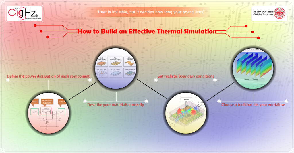
A simulation is only as smart as the data you give it. It doesn’t guess; it calculates. So, accuracy starts with setup.
Step-1
First, define the power dissipation of each component. Use real numbers from datasheets or circuit calculations.
If a voltage regulator dissipates 1.5 watts, don’t just round it off — that value shapes the entire heat map.
Each part on your board is a heat source, and the simulation needs to know how strong each source is.
Step-2
Next, describe your materials correctly. FR4, aluminum, and ceramic substrates all behave differently when it comes to heat conduction.
Copper thickness, layer count, and dielectric type affect how heat spreads through the stack.
Even solder mask thickness can slightly change how heat escapes to the environment.
Step-3
Then, set realistic boundary conditions. In the real world, your PCB doesn’t float in open air.
It sits inside an enclosure, maybe near a battery, maybe under a fan.
Add those conditions to the model. Airflow direction, enclosure walls, and mounting orientation — they all influence how quickly heat leaves your system.
Step-4
Finally, choose a tool that fits your workflow. Many PCB design tools today have built-in thermal solvers — Altium Designer, Fusion 360 can all run meaningful simulations.
For detailed results, software like ANSYS Icepak Flow gives full thermal field analysis.
The goal isn’t fancy visuals, but clarity — to see how every watt of heat travels through your board.
Reading the Results — What They Actually Mean
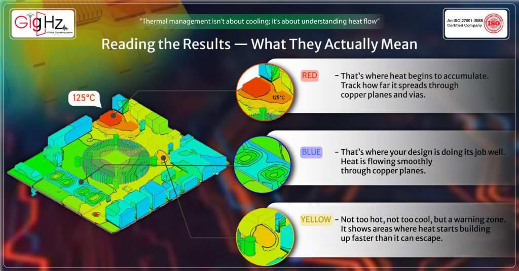
Once the simulation finishes, the screen fills with colors — cool blues, warm reds, and bright yellows showing temperature zones.
But don’t stop at looking; interpret what those colors are telling you.
A small red spot under a power IC might not seem dangerous, but that’s where heat begins to accumulate.
Track how far it spreads through copper planes and vias. Notice whether the temperature stabilizes or keeps rising over time.
These trends reveal whether your board can handle real operating conditions.
A blue zone might look calm and safe — and it usually is. That’s where your design is doing its job well.
Heat is flowing smoothly through copper planes, and components in this region are staying within a comfortable temperature range.
Then comes the yellow region — not too hot, not too cool, but a warning zone.
It shows areas where heat starts building up faster than it can escape. These are often near voltage regulators or switching components, where energy conversion happens.
Watch these spots closely — they tell you where thermal bottlenecks might begin.
Also, compare results with datasheet limits. Every component has a maximum junction temperature, often around 125°C or 150°C.
If your simulation shows a steady-state rise approaching that range, it’s a warning — not for failure today, but for reliability loss tomorrow.
Run both steady-state and transient simulations. Steady-state tells you how the board behaves after running for hours, while transient shows short bursts — power-up, high-load switching, or startup surges.
Real circuits experience both, and understanding both helps you plan better cooling.
Improving the Design After Simulation
Once you know where the problem lies, the next step is fixing it inside your layout — not by adding fans, but by designing smarter.
- Start with copper.
- It’s your best passive heat spreader.
- Use thicker copper layers wherever current is high, and ensure power and ground planes are wide and continuous.
- Avoid narrow copper islands that trap heat in one spot.
Then add thermal vias — small, plated holes that carry heat from one layer to another.
Placing them under power components like regulators or FETs helps transfer heat to inner or bottom layers.
A grid of properly placed vias can lower junction temperature significantly without any extra cost.
Next, look at placement. If heat-sensitive components like sensors or oscillators are sitting too close to heat-generating ICs, move them apart.
Keep power components near airflow paths or open edges of the board.
Sometimes, shifting a single regulator by a centimeter can balance the temperature across the board.
Trace width also matters. Power traces act like both electrical and thermal conductors.
Wider traces reduce resistance and also carry heat more evenly. For high-current paths, a few extra millimeters in width can make a measurable temperature difference.
And finally, consider airflow. If your board sits in a case or enclosure, study how air actually moves inside it.
Direct the airflow across the hottest zones instead of letting it pass unused space. In many cases, improving ventilation gives better results than adding extra copper.
Validating Your Simulation in Real Life
Even the best simulation is still a prediction. To close the loop, test your real prototype.
Use a thermal camera or thermocouples to measure actual temperatures at critical points. Compare them with your simulation map.
If you find a difference, don’t ignore it — update your model. This process makes your future simulations more accurate and more valuable.
Thermal design is not a one-time task. It’s a continuous cycle of predicting, testing, and refining.
The more feedback you build from real boards, the more your next design will behave exactly as your model predicts.
Bottom Line
Heat is invisible, but its effects are permanent. Every overheated trace, every stressed solder joint, quietly reduces the life of your product.
That’s why managing heat is not just about preventing failures — it’s about designing for long-term reliability.
thermal management in PCB gives you vision. It shows you what’s happening beneath the layers and helps you make smarter choices.
where to place power components, how to spread copper, how to use vias, and how to plan airflow.
When you handle heat early, your design becomes stable, durable, and trustworthy.
So, before you route your next PCB, take a few minutes to run a thermal simulation.
Look at the heat flow. Fix one hotspot. Those small changes today prevent big problems tomorrow.
Book a Call. Schedule a Free Consultation now https://calendly.com/gighz/30min
Stuck in a loop of challenges? Always pick smart solution that works
Have you faced costly rework because 2D drawings skipped in MCAD workflows?
Effective way to prevent MCAD documentation errors recalls?
Please answer both poll questions before submitting.
Thank you for your response! 😊
Latest Post
Get Customized Engineering CAD Design Service

Book a Free Consultation Call
Partner with Gighz and bring your most innovative design concepts to life. Our engineering cad services accelerate development so you can focus on your big vision.