

5 PCB Design Constraints That Can Conflict in Real Designs
- Posted On:
- November 13, 2026
- Category:
- Ecad

A PCB layout rarely fails because one requirement was ignored. More often, two valid requirements pull the design in different directions.
A high-speed interface may need wider spacing, while routing density demands compact traces. A power component may need to stay close to its load, while thermal management calls for more separation. Mechanical and manufacturing limits add further constraints.
These conflicts can affect signal integrity, power delivery, EMI, thermal performance, and manufacturability.
Here are five common PCB design constraints that can conflict in real designs.
Where PCB Design Constraints Start to Conflict
Most PCB constraints look reasonable separately. The difficulty appears when they affect the same component, routing channel, copper region, or layer.
For example, increasing trace spacing may improve signal integrity but reduce routing space. Moving a power component may improve thermal separation but increase current-loop area.
These trade-offs usually become visible during placement and routing, so critical constraints should be identified early.
1. Signal Integrity vs Routing Density
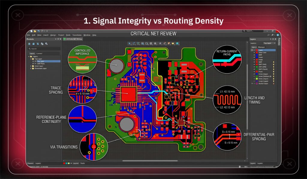
High-speed signals need controlled impedance, suitable spacing, continuous reference planes, and carefully managed layer transitions.
On a dense board, these requirements compete with available routing space.
Increasing spacing between high-speed traces can reduce crosstalk, but it consumes routing channels. Avoiding vias can reduce discontinuities, but may force longer routes or make routing impossible.
Layer changes create another concern: the return current needs a low-impedance path through the reference structure. If the reference plane changes or is interrupted, the return current may take a longer path, increasing loop area and potentially degrading signal quality.
What to check
For critical nets, review:
- Controlled impedance
- Trace spacing
- Reference-plane continuity
- Via transitions
- Return-current paths
- Length and timing requirements
- Differential-pair spacing
The goal is to find an electrically suitable route that fits the available routing space.
2. Power Integrity vs Thermal Performance

Power delivery creates a different trade-off.
High-current paths benefit from short connections, wide copper, multiple vias, and low-inductance paths. This help reduce voltage drop and power-distribution impedance.
At the same time, power components can generate substantial heat.
Consider a switching regulator. The input capacitor, switching device, and other components in the high di/dt loop need to be close together. Increasing their distance may improve physical separation, but it also increases loop area and parasitic inductance.
Thermal performance depends on copper spreading, thermal vias, component spacing, airflow, and the connection to the enclosure.
What engineers should evaluate
Check:
- PDN impedance and voltage drop
- Current density
- High-frequency loop area
- Component temperature
- Thermal-via effectiveness
- Heat-spreading paths
A good power layout balances electrical performance with thermal behavior.
3. EMI Control vs High-Speed Routing
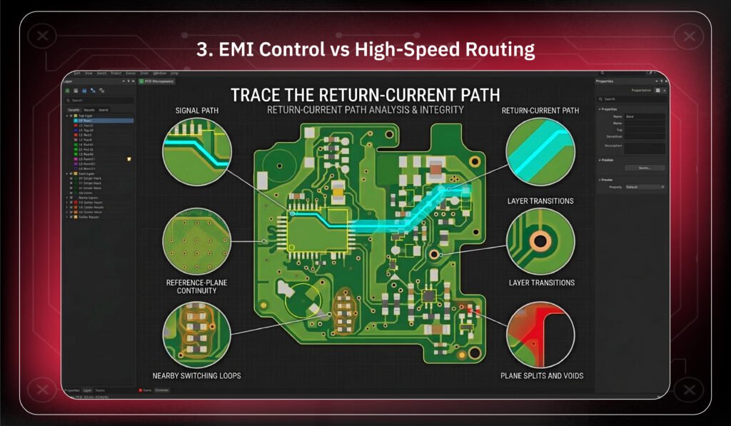
EMI becomes difficult when fast signals and noisy circuits share limited board area.
Switching regulators, clocks, and other fast-changing signals can generate unwanted coupling. Large current loops and poor return paths can make the problem worse.
Increasing separation between an aggressor and a sensitive signal can help, but there may not be enough routing space.
Moving the signal to another layer may solve the spacing problem while creating a return-path discontinuity.
That is why EMI-aware routing requires more than physical separation.
Follow the current path
For sensitive or high-speed nets, check:
- Signal path
- Return-current path
- Reference-plane continuity
- Layer transitions
- Nearby switching loops
- Plane splits and voids
A route that looks clean can still create EMI problems if its return current has no suitable path.
4. Compact PCB Layout vs Manufacturability
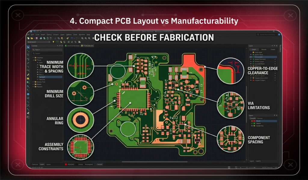
Reducing board size can quickly affect manufacturing.
A compact layout may require narrower traces, smaller vias, tighter component spacing, and reduced copper clearances.
Each change improves routing density while reducing manufacturing margin.
For example, a smaller via may free routing space but require tighter fabrication capabilities. Tighter component placement can save board area but make assembly, inspection, or rework more difficult.
Check the actual manufacturing capability
Before using aggressive layout features, confirm:
- Minimum trace width and spacing
- Minimum drill size
- Annular ring requirements
- Copper-to-edge clearance
- Via limitations
- Component spacing
- Assembly constraints
The CAD rule set is not the same as the manufacturing capability.
DFM checks should happen before the layout becomes dependent on extremely tight features.
5. Component Placement vs System Requirements
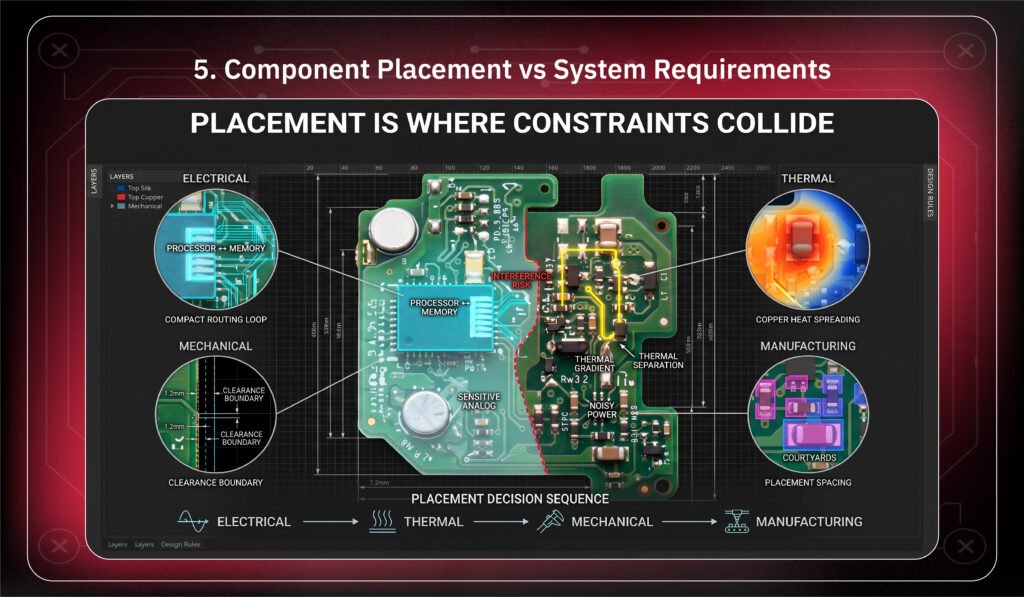
Component placement is where many PCB constraints first collide.
A processor may need to be close to memory. A switching regulator may need to remain close to its load. Sensitive analog circuitry may need separation from noisy power sections. Connectors may have fixed mechanical positions.
Thermal requirements add another constraint.
A high-power device may need copper area or airflow, while a sensitive component may need to remain away from that heat source.
Moving one component can affect several design objectives.
For example, moving a power converter away from an analog section may reduce noise coupling but increase power-loop length. Moving memory closer to a processor may improve routing but increase local thermal density.
Make placement decisions early
Before committing to placement, consider:
Electrical → Thermal → Mechanical → Manufacturing
The objective is to create a placement strategy that gives the entire board enough room to meet its critical requirements.
How to Manage Conflicting Design Constraints
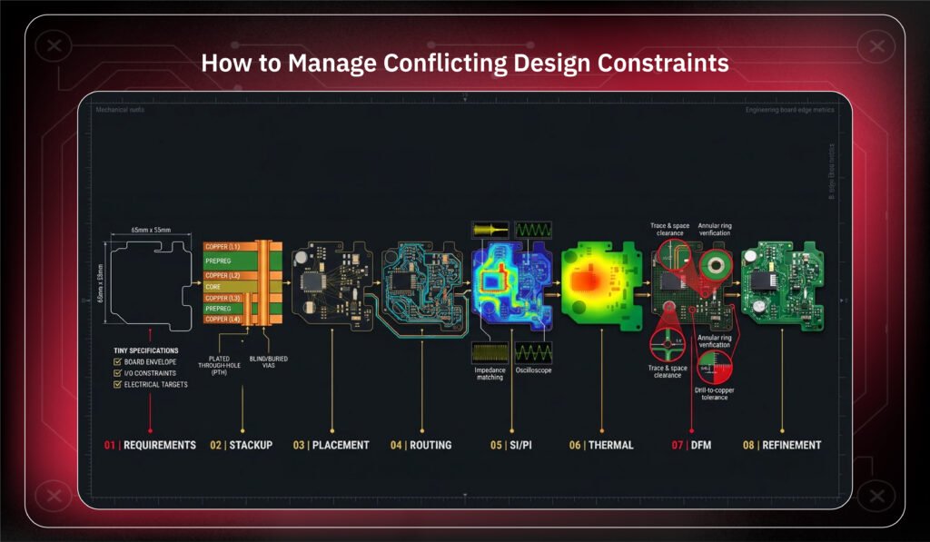
When constraints conflict, protect the most critical requirement first and identify where flexibility remains.
For example, prioritize impedance and return paths for high-speed signals, critical current loops in power circuits, and fabrication limits on compact boards.
A practical flow is:
Requirements → Stackup → Placement → Routing → SI/PI → Thermal → DFM → Refinement
If analysis finds a problem, revisit the relevant design stage before fabrication.
Final Answer
Real PCB design is rarely about optimizing a single parameter when dealing with PCB design constraints.
Signal integrity, power delivery, EMI, thermal performance, mechanical size, and manufacturability all compete on the same board.
The goal is not to maximize every constraint.
It is to identify which constraint matters most in each area, make deliberate trade-offs, and validate them before fabrication.
A PCB that passes DRC is not necessarily reliable in practice.
Good design comes from balancing electrical, thermal, mechanical, and manufacturing needs—not treating them separately.
Optimize critical layout decisions—get your design evaluated.
Book a Call. Schedule a Free Consultation now. https://calendly.com/gighz/30min
Frequently Asked Questions
- Why are vias important in high-speed PCB design?
Vias can introduce parasitic, impedance discontinuities, and signal reflections. - What is a via stub?
An unused barrel section that can cause reflections and resonance. - When is back drilling needed?
When a via stub becomes electrically significant to the signal. - Why is the return path important?
An interrupted return path can increase EMI, crosstalk, and signal-integrity issues. - Does DRC guarantee reliable vias?
No. Critical vias may require SI analysis to verify electrical performance.
Stuck in a loop of challenges? Always pick smart solution that works
Have you faced costly rework because 2D drawings skipped in MCAD workflows?
Effective way to prevent MCAD documentation errors recalls?
Please answer both poll questions before submitting.
Thank you for your response! 😊
Latest Post
Get Customized Engineering CAD Design Service

Book a Free Consultation Call
Partner with Gighz and bring your most innovative design concepts to life. Our engineering cad services accelerate development so you can focus on your big vision.
